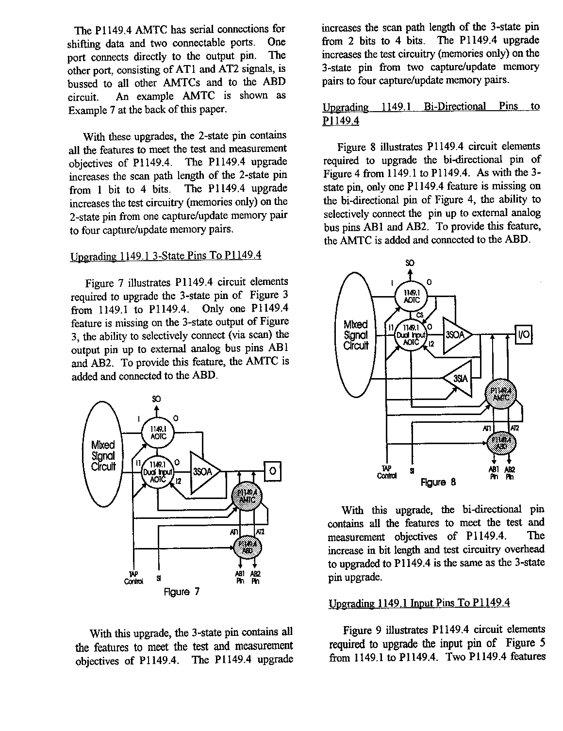
for
October 22, 1995
| Time | Topic | Responsibility |
|---|---|---|
| 8:00am | Arrival and introductions | Adam Cron |
| 8:15am | Approval of May, 1995 minutes | Adam Cron |
| 8:30am | Presentation of the proposal made to 1149.1 | Lee Whetsel |
| 9:30am | .1/.4 overlap strategy/positioning | Gordon Robinson Ken Parker |
| 10:00am | Break - Thank you Hewlett-Packard | |
| 10:30am | 1149.1/P1149.4 overlap - continued | |
| 11:00am | AB/AT switches (calibration suite) | Steve Sunter Brian Wilkins |
| 11:45am | Patent follow-up | Mani Soma |
| 12:00pm | Lunch - Thank-you Hewlett-Packard | |
| 1:00pm | Variable Vref - How might we support it? | Lee Whetsel Steve Sunter |
| 1:45pm | Differential cells | Steve Sunter |
| 2:30pm | IIC - Formal Response | Frans de Jong |
| 2:45pm | IC progress report | Keith Lofstrom |
| 3:00pm | Break - Thank you Hewlett-Packard | |
| 3:30pm | Internal Control Cells | Charles Meyerson |
| 4:15pm | Draft D05 progress report | Brian Wilkins |
| 5:00pm | Cost calculations for adding P1149.4 | Steve Sunter |
| 5:20pm | Balloting schedule | Adam Cron |
| 5:40pm | 1149.n updates | Anyone |
| 5:55pm | Next meeting in Scotts Valley, CA in February, 1996 | Adam Cron |
| 6:00pm | Adjourn | Adam Cron |
| Working Group Members | 35 |
|---|---|
| Total Subscribers | 257 |
| Countries Participating | ~23 |
| Companies Participating | ~158 |
| Funds Available | $2219.99 |
| Name | Company Sponsor |
|---|---|
| Terry Borroz | Teradyne, Inc. |
| Bill Coombe | Medtronic |
| Bernard Courtois | Institut National Polytechnique de Grenoble |
| Adam Cron | Motorola |
| Dan Dandapani | University of Colorado |
| Frans de Jong | Philips Electronic Design & Tools |
| Steve Dollens | International Microelectronic Products |
| Tom Fisher | Delco Electronics |
| Allen Heiden | Motorola |
| Madhuri Jarwala | AT&T Bell Laboratories |
| Terry Junge | Seagate International |
| Jake Karrfalt | Alternative System Concepts |
| Mehdi Katoozi | Boeing |
| Keith Lofstrom | KLIC |
| Colin Maunder | British Telecom |
| Charles Meyerson | Medtronic |
| Benoit Nadeau-Dostie | LV Software Canada Inc. |
| Naveena Nagi | LogicVision |
| Elbert Nhan | Johns Hopkins University |
| Stig Oresjo | Hewlett-Packard |
| Ken Parker | Hewlett-Packard |
| Michel Parot | Thomson-CSF |
| Gordon Robinson | GenRad |
| Mani Soma | University of Washington |
| Steve Sunter | Nortel |
| Lee Whetsel | Texas Instruments |
| Brian Wilkins | Southampton University |
| Name | Company Sponsor |
|---|---|
| John Andrews | National Semiconductor |
| Nai-Chi Lee | Philips |
The Working Group thanked Hewlett-Packard for sponsoring this meeting.
Stig Oresjo announced he is retiring from the P1149.4 Working Group
but will continue working with the Working Group on P1149.4 manufacturing
issues. Stig presented the Working Group with a formal resignation
letter wishing us "all the luck in the future".
Gordon Robinson motioned to thank Stig for his work with P1149.4. Seconded.
Unanimous approval.
Adam Cron motioned to approve the May, 1995 minutes. Seconded. Unanimous
approval.
Lee Whetsel's Presentation to 1149.1.
Brief background: At the Portland Oregon P1149.4 meeting Lee mentioned
he'd been working on simple 1149.1 compliant analog cells that don't have
measurement circuitry and AB1&2 pin requirements. Lee suggested P1149.4
make these cells and the 4 pin TAP they require the baseline for P1149.4,
to address interconnect testing of pin limited ICs. P1149.4 rejected this
suggestion since P1149.4's objective is for full analog testing using the
currently defined cell and 6 pin TAP interface. Lee told P1149.4 he was
going to propose the simple cells to 1149.1. P1149.4 endorsed this action
by Lee. At the Portland Maine 1149.1 meeting, Lee presented the simple
analog cells for the first time. They were well received by 1149.1. At
ITC, Lee repeated the cell presentation to P1149.4 accompanied by a paper
detailing how 1149.1 and P1149.4 could cooperatively develop a Mixed-Signal
Test Bus Standard.
REFER TO LEE'S VIEWGRAPHS:
Figure 1 shows the current 1149.1 requirements
for mixed-signal boundary-scan (one test cell is required for each digital
I/O and n test cells are required for each analog I/O; at least 4 pins
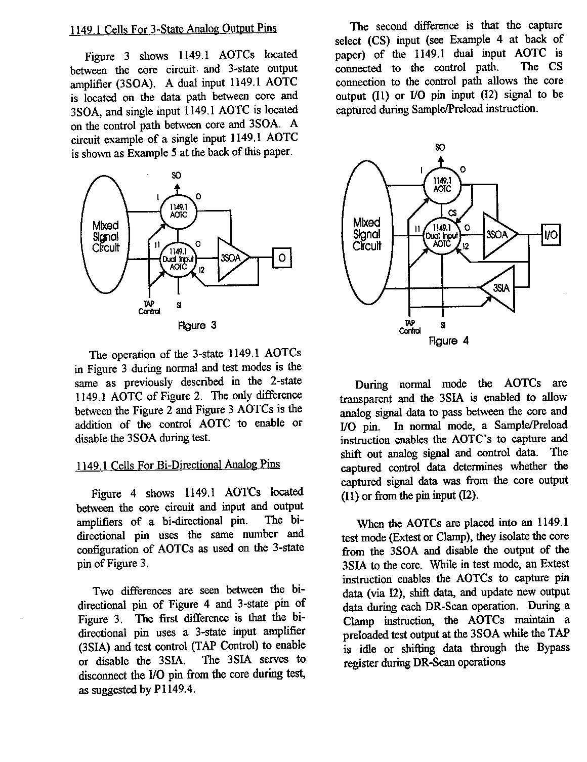
for the test bus). Figure 3 illustrates the
test method using the current 1149.1 structure (2 test cells for each digital
interconnect and 2 groups of n test cells for each analog interconnect).
Figure 2 presents the likely future mixed-signal
boundary-scan scheme for P1149.4 (only one test cell is required for each
digital or analog I/O, and the test bus requires at least 6 pins). Figure
4 shows when using the P1149.4 test method, one would need only 2 test
cells for each digital or analog interconnect. Figure
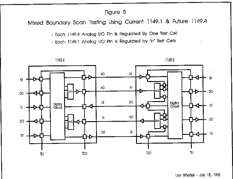
5 combines the current 1149.1 structure with future P1149.4 structure
which means each P1149.4 analog I/O pin would be regulated by 1 test cell
while each 1149.1 analog I/O pin would be regulated by n test cells. Figure
6 reconciles the difference between 1149.1 and P1149.4 by making each
P1149.4 AND 1149.1 analog I/O regulated by 1 test cell with an option for
partitioning. One test cell is now needed on 1149.1 analog I/O pins to
control and observe data.
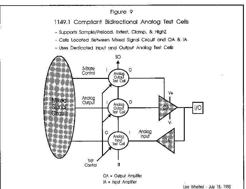
Figures 7, 8,
and 9 represent 1149.1 compliant 2-state and
3-state output analog test cells, as well as bi-directional test cells.
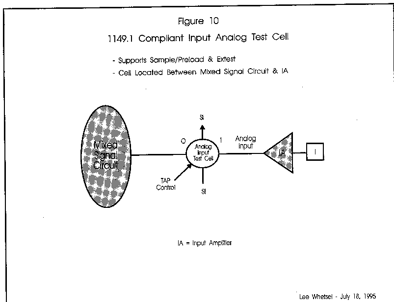
Figure 10 shows a 1149.1 compliant analog input
test cell. Figures 10 and 11
detail the 1149.1 compliant analog input and output test cells, respectively.
Figure 13 shows how 2 analog output cells may
be connected between the mixed signal circuit and the pin, and still comply
to 1149.1. The details of the cells in Figure 13
are shown in Figure 14.
Ken had a question about Figure 13's S2 and
S3 "small" switches; full capability of the pin driver is still
available. Mani Soma asked if V+ and V- is programmable. The answer is
whatever voltages it takes to make the output go to Vmin and Vmax. Mehdi
commented that if an analog circuit is connected to a digital circuit,
the minimum and maximum excursions of the analog voltages could hurt the
digital circuit. Steve Sunter said this is just an implementation example.
In Figure 12, the switch is conceptual.
Figure 13 shows optimized 1149.1 compliant
bi-directional analog test cells. This scheme simulates 1149.1 bi-directional
test cells. Colin Maunder cautioned that we not only need to be concerned
with "low level" tests, but also a "higher level" of
testing. Lee said this is 1149.1's way of testing simple interconnects
and shorts, but Colin disagreed. Adam interjected that Lee's proposal is
to implement how 1149.1 is doing test (to make a clean break between 1149.1
and P1149.4), and P1149.4 's job, according to Lee, is to complete the
scheme for mixed-signal testing. Ken commented that Lee's proposal is just
to test simple wires and interconnects, but Colin said we need to be clear
on how to test all kinds of components, not just simple wires. Colin said
SAMPLE/PRELOAD instructions are for logical level tests only. Ken explains
when an P1149.4 chip is trying to "listen to" an 1149.1 chip,
at this moment there is no way to do that unless one implements Lee's scheme
or some other method. Mani asked, when Lee presented this to 1149.1, what
the reaction/response was. Lee Whetsel said 1149.1 readily embraced it
but Gordon Robinson proposed forming a study team to discuss this subject.
Overall, the response was favorable.
Next, Lee showed viewgraphs of the diagrams found in his 9/21/95 paper
entitled "Proposal to Simplify Development of a Mixed Signal Test
Standard." Figure 1 in the paper presents analog
output/input test cells that exist between mixed signal circuit input/output
pins. The cells can be as simple as two switches and a TAP control. Figure
2 is a diagram of a possible 1149.1 2-state cell (full-time drive and
not tri-statable) between the mixed signal circuit and an output pin. An
improvement can be made to this cell by feeding the output back to the
cell for observing. Figure 3 is basically identical
to Figure 2 except another cell is added to control
the 3-state output amplifier (3SOA); an example of the cells is similar
to Figure 11 in Lee's viewgraphs of the proposal
made to 1149.1. For bi-directionality, just add a 3-state input amplifier
(3SIA) to the structure in Figure 3. Ken said the
scheme presented in Figure 3 is sufficient for most
bi-directional purposes unless one needs to put the circuit into a quiescent
state. Figure 5: For inputs, use one 1149.1 AITC
as a capture cell. The 3SIA is used during test mode to isolate input signal
data from the core and allow the AITC to capture and shift out analog signal
data at the input pin. Figure 6: The shaded blocks
are what P1149.4 needs to make its measurements. There were comments on
the need to have clear descriptions of instructions. Questions were raised
about the need for 3SIA/3SOA because sometimes only passive components
are hanging at the pin. Ken reminded that Lee's presentation is predicated
on testing simple wires and interconnects. Lee said this is a "what
if" presentation. What if you have 1149.1/.4 chips talking/listening
to each other, then what are the cells/circuitry required by P1149.4 to
do P1149.4 measurements? Figure 7 shows how to upgrade
1149.1 3-state pins to P1149.4. Again, the shaded blocks are what P1149.4
needs to complement 1149.1 3-state circuitry which only provides 1, 0,
and disable. Figure 8 is for bi-directionality.
Figure 9: upgrading 1149.1 inputs to P1149.4. This
is by far the most expensive upgrade of all since 1149.1 only provides
an 3SIA, and we also need the rest of the structure for P1149.4 measurement
capabilities.
Adam commented that he has concerns about 4 pins vs. 6 pins. We might
not have chips with 6 pins (P1149.4) out there if developers can only afford
4 pins (1149.1). But one never knows. Madhuri said Lee's schemes might
not be useful since they are only for testing simple wires. Keith Lofstrom
commented that when adding all this additional circuitry, there may not
be enough drive. The 1149.1 by itself doesn't drive but the upgrade version
does (Figure 9). Brian Wilkins agreed with Lee's
proposal. The problem is what we can assume about what 1149.1 will include
in its standard. The worst scenario is that we have to throw away the current
P1149.4 draft. Miscellaneous comments that P1149.4 will not allow partitioning.
Colin reiterated that we must understand what we are doing (testing)? We
would need to break our objectives down one by one and put the bits and
pieces together. Ken said that was why few years ago, he advocated putting
1149.1 on all pins and optionally P1149.4 layer can be added as needed.
Adam summarized: Just focus on capabilities, not on the number of bits.
Be general and flexible. We need to keep going with what we're doing since
1149.1 has not voted on Lee's proposal.
Steve said that if you want analog G, it must be the P1149.4 "G",
not 1149.1 logic 0, since 1149.1 does not have sufficiently stable or enough
drive in some instances. Lee said he thinks 1149.1 should accept his proposed
test cells as a requirement on every pin. Gordon commented that the highest
level of testability is P1149.4 today on pin by pin basis. He outlined
4 levels of testability: 1) does nothing, 2) 1149.1 capability, 3) analog
1149.1 capability, or 4) full P1149.4 capability. Designers should be allowed
to use any of these on a pin by pin basis. Colin said we should decide
which instructions should be mandatory and which are mandatory only in
certain cases. Colin advocated establishing a much clearer definition of
"EXTEST". His opinion is that EXTEST should include more than
just simple interconnect test. Madhuri again voiced concern that Lee's
proposal only covers the simple cases of wires & shorts. His proposal
would test maybe 50 to 70 % of all analog interconnects. Steve said we
can extend 1149.1's definition of logic high/low to Vmax/Vmin. There are
3 options: 1) no boundary scan, 2) 1149.1, and 3) P1149.4. In 1149.1 chips,
make 1149.1 capability on analog pins optional. In P1149.4 chips, all P1149.4
pins must have 1149.1. Gordon suggested motioning joint 1149.1/P1149.4
members to propose changes to 1149.1. Brian agreed there is a need for
a clear definition of 1149.1 test. Perhaps we should quit talking about
putting 1149.1 or P1149.4 on this or that pin.
SUMMARY: Lee discussed the proposal of changes to be made in
1149.1 presented to the 1149.1 Working Group in July. The response of 1149.1
so far seemed favorable but no action has been taken on it. In the P1149.4
Working Group, there was both support for and opposition to the concept
of pin-by-pin classification. There were concerns about the practicality/usefulness
of Lee's proposal as it only covers simple interconnects.
1149.1/P1149.4 overlap.
Ken motioned to invite 1149.1 Working Group members to discuss joint
1149.1/P1149.4 issues sometime in the future. Seconded. Discussion followed.
We should do as much as we can at this meeting and at the 1149.1 meeting
on Thursday. They (1149.1 Working Group) may decline our invitation. Steve
openly worried about implications of such a joint meeting, because we would
end up discussing only digital issues. Suggestion that this could be a
different meeting from the Scotts Valley meeting. Lee proposed having a
meeting SOON to achieve real progress. Ken said he would love to see progress
but thought that we are still far away from balloting.
Gordon pointed out there are 2 simple issues. Let's get a group decision
on where to start. If we can arrive at common grounds on what we want,
then on Thursday, we can raise it at the 1149.1 Working Group meeting.
We need, at that point, to have everyone in 1149.1 involved and vote on
the relevant issues. Maybe a 1149.1/P1149.4 meeting can be arranged for
2 hours. Colin suggested to break into little subgroups and focus on specific
issues and have the subgroups report back to our Working Group. Gordon
said let's make assumption to have a group meeting and let's make it clear
which issues we're disagreeing about and only then it makes sense to have
the meeting. People who felt strongly about the issues should make the
meeting. As a result, a revised motion was on the table for having a joint
1149.1/P1149.4 meeting between after 6:00PM today and sometime during ITC.
Gordon suggested getting 6 people to get together and work on a specific
set of proposals before the 1149.1 meeting on Thursday. Lee said he would
like to recommend to 1149.1: Let 1149.1 do the digital part of P1149.4
(update/capture); a required feature of the infrastructure on 1149.1 chips.
Then there was discussion about level of revision of BSDL for old and new
chips (i.e. A-compliant, B-compliant, or C-compliant).
Ken withdrew the previous motion now that a small subgroup will soon
be formed to work on proposing to the 1149.1 on Thursday. Adam asked who
would like to be in the subgroup: Steve Sunter, Colin Maunder, Brian Wilkins,
Lee Whetsel, Ken Parker, and Madhuri Jarwala.
SUMMARY: The Working Group decided, after deliberations, to form
a small subgroup to outline 1149.1/P1149.4 issues that would be presented
to 1149.1 at the 1149.1 Working Group meeting on Thursday. The idea is
to make recommendations to 1149.1 based on Lee's proposal to have changes
in the 1149.1 Standard made so that P1149.4 would be compatible with 1149.1.
AB/AT calibration suite (Refer to Steve Sunter's handouts).
Steve put up a viewgraph which contained basically what Brian put in
the draft with a little modification. In viewgraph
1 (Connecting AT pins to AB buses), item (i): Steve recommended not
to leave the internal analog test bus in high-impedance state (good design
practice but not essential for proper P1149.4 operation). It should not
be a requirement (that's why the word "should"). Colin asked
what it is we are trying to achieve with this recommendation. He said we
should not describe a way to get there. Steve replied that it's just a
note. Mehdi was concerned about how disconnecting AT and AB busses would
affect the operation of other chips. Ken said by definition, core disconnect
implies no effect on other chips. After more debating, it was agreed that
(i) be deleted.
Item (ii): Modified to read: "It shall be possible to electrically
connect and disconnect each internal analog test bus line (AB1 and AB2)
to its corresponding ETAP pin (AT1 and AT2 respectively)." Colin commented
that the wording "connect" and "disconnect" imply implementation
details involving switches which may not be the only way to implement it.
Steve responded by saying let's make the switches conceptual. Ken asked
how about changing to "isolate electrically". The final consensus
was to leave it to Brian to work out the wording.
Item (iii): Modified to read: "It shall be possible to provide
a path from the AT1 pin to the AT2 pin, without enabling other connections
to permit testing of the AT1 and AT2 buses." The motivation is to
allow the integrity of the bus infrastructure (wire paths on-chip and off-chip)
to be verified. Colin said what if the 2 buses are swapped, there is no
way to find out at this moment. After discussions, "AT1 & AT2",
the board level busses, were added between the words "the" and
"buses" as shown above. Colin said maybe we need to define what
the specific instruction is to do this with. Steve said let's defer the
discussion on specific instructions since we may have 3 or 4 separate instructions
that require (iii). The words "internal voltages" mean the AB
busses are connected to internal voltage references, according to Mehdi.
So "to the pins or internal voltage" was taken out. The original
motivation for the deleted phrase was to allow designers' ad-hoc connections.
Dan suggested that since all these are instruction-related, perhaps we
should wait until discussion of instruction to vote on these items. Keith
asked if the Working Group could discuss instructions now so that we can
be in the position to act on Steve's recommendations. However, Steve preferred
to continue with what he has and defer on motioning.
Item (iv): Ken said we might not need both G and +V for calibration
purpose. AT1 can be treated as an 1149.1 analog input and AT2 as an 1149.1
analog output. AT1 will meet requirements for 1149.1 analog input, while
AT2 will meet requirements for 1149.1 output analog output. Therefore,
AT1/AT1 comply with 1149.1 (under EXTEST?). It soon became clear that this
item will have to be revisited sometime in the future.
SUMMARY: (Refer to Steve Sunter's viewgraph
1) The WG agreed (i) is just a note and will be modified by Ken Parker
in the afternoon. Items (ii) & (iii) are agreed upon as capabilities
and (iv) tabled for discussion later.
Ken Parker 's unscheduled presentation.
Ken initiated a motion which is referenced to Steve's (i) discussed
this morning in his viewgraph 1.
MOTION: Given the ability to disconnect ABn from ATn, the state
of ABn shall have no effect on either the normal or test operation of the
device when ABn is disconnected. Motion was amended by deleting the phrase
"the state of" as suggested by Lee Whetsel. Note: AB is internal
bus of device and AT is the external bus to pin. Motion was seconded. Aye:
16. NO. 0. Abstention: 1. Motion carried.
Referring to handout of e-mail with subject "Last
minute mail...". This is functionally equivalent to Brian's scheme
in the draft D05 Figure 10. However, this design is not compatible with
existing 1149.1 software and doesn't meet definition of BYPASS and SAMPLE.
This design is also not an "idiot-proof" scheme (people might
do things to the flip-flops which can affect the pins even though we are
in the BYPASS mode). A modified Figure 10 of
the same ABM is shown on the reverse side of Ken's Figure 10 handout. It
has a self monitoring output cell. CAPTURE/UPDATE flip-flops are by definition
boundary-scan cells. The TAP has a new output called AFUNC. The interesting
thing is that in EXTEST mode, the S1 and S2 switches are for data and enable
in pseudo 1149.1 test mode, and if neither is on, then it's tri-state.
Now in parametric test, we can enable AB1 and AB2. The same EXTEST instruction
can control both pseudo-.1 test and parametric test. This supports 1149.1
software, meets BYPASS & SAMPLE rules and implements analog SAMPLE,
etc. In effect, Ken is proposing that EXTEST has the dual role (expansion
of definition) of pseudo-.1 and parametric tests. Try to keep the instruction
count as low as possible. In addition, with this design, one can do other
things off-chip.
Question: If we took AB1 and AB2 and the last bit (flip-flop Z) out
of Ken's ABM, are we left with something similar to Lee's proposal? Ken
said there are other simplifications such as merging the AND gates into
the driver. Adam asked Ken if he is showing the implementation details
with his diagram? Ken said Figure 10 of Brian's draft is inconsistent with
what's been said and he is trying to make the little changes to make it
consistent. This is indeed an implementation example. What we should be
able to do is to write down a set of rules based on this example without
showing it.
Ken's initial definition of EXTEST: Both pseudo-.1 and parametric tests.
A lot of integrity checking goes on during normal chip operation, at least
in 1149.1. So, we need an integrity checking function to check the chip.
We don't need a separate EXTEST instruction to check the integrity of AT
busses. This diagram will not be part of the Standard, but stands as an
example. We need nomenclature for the "X", "Y", and
"Z" flip-flops (memory elements) for the Standard.
A question arose as to whether one can fan-out the enable control bit
to other pins to save some bits. The answer is "no" since one
may want to independently control switches at each pin. However, 1149.1
allows paralleling the pins. This is a typical example of P1149.4 and 1149.1
not merging smoothly. Steve Sunter suggested to vote on this. But Ken said
someone should double check his work. Steve said he completely agrees with
Ken's scheme because it's consistent with previous work Steve had done.
A motion was on the floor to vote on the acceptance of the 4 operations
in Ken's design. MOTION: Adopt definitions of instructions per Ken
Parker's e-mail dated 10/20/95 and presentation
verbiage as supported by circuit diagram. Seconded.
Aye: 17. Nay: 0. abstention: 0. Unanimous approval.
SUMMARY: Ken Parker presented a modified
analog boundary-scan design of the one in Draft D05 to minimize the
instruction count. The new design allows one EXTEST instruction, the definition
of which was expanded, for both 1149.1 and P1149.4 tests.
Steve Sunter's variable Vref.
Refer to Steve's handouts for the following discussion. Viewgraph
2: We've agreed to include an optional variable Vref and mandate one
which is constant-level. Ken had problem with the second tick under the
first bullet. Steve agreed to cross it out. He also deleted the third tick
mark. Vmin and Vmax are pin specific. After some debating, the following
motion was on the floor.
MOTION: For each pin there shall be a mandatory DC Vref, between
Vmin and Vmax. Seconded. Aye: 17. Nay: 0. Abstention: 1. Motion carried.
For the second bullet on the same viewgraph 2,
Steve asked the Working Group to agree to the motion that variable Vref
may be connected but how it's connected can be discussed later. Further
discussion resulted in brackets being put around the two tick marks underneath
the bullet. The proposal is: Yes, we'll make provision for a variable Vref.
This is to allow for cases where Vref needs to be adjusted for proper operation.
Mehdi questioned if we are accomplishing anything by passing this motion
because the reference can come from off-chip and can be programmed to anything
we wanted. But Steve said this is just for having Vref. The discussion
quickly turned into that of the conceptual comparator. Mehdi actually was
concerned about the possibility of the Vref being interpreted as an actual
bandgap on-chip reference. Ken said to think of it as a 1-bit A/D. Ken
asked what instruction we are talking about here. If EXTEST, then we must
have a Vref. Lee suggested getting rid of the word "Vref." Adam
urged the Working Group to just talk about the concept, not the actual
wording which will be taken care of by Brian in the draft.
Dan said just to call it a 1-bit A/D, but Steve said this is not addressing
the fact that we need a level above which we can call high and below which
we can call low. Tom Fisher said this is not a conceptual function, it's
a REAL function. Steve said the issue here is whether we should have a
fixed Vref and/or variable one. Mehdi originally initiated a motion on
this proposal but later withdrew it.
SUMMARY: A motion was passed to mandate the existence of a constant-level
Vref between Vmin and Vmax at each pin for test purposes. Provision was
made for the capability to adjust the Vref level as necessary.
Steve Sunter's differential pins.
The reason for differential pins is to make
accurate measurements in spite of noise. The possibility of reducing area
also exists. A question might be: Can differential measurements be made
with only 2 wires. The answer is "yes." Steve stipulated that
we need identical signal paths for AB1 and AB2. If accuracy is not needed,
use single-ended testing. Are the benefits worth 2 extra analog bus pins?
Only for ICs with lots of differential pins. How different are 2 and 4
wire switch schemes? Same, except drive pins to opposite logic levels in
interconnect mode.
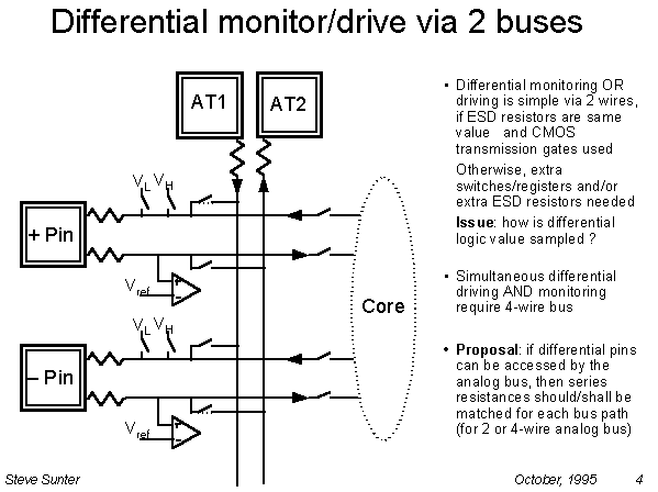
Viewgraph 4: Both resistors must be matched
for the 2 paths to appear the same during test. However, these resistors
need not be in the path during normal operation. Proposal: If differential
pins can be accessed by the analog bus, then series resistances should
be matched for each bus path (for 2- or 4-wire analog bus). Ken said the
Standard should provide guidelines for designers since designers may not
have thought of all of the implications. Steve mentioned that this matched-resistor
design is consistent with Kelvin measurement which was discussed in the
last Working Group meeting. The driving path should be different from the
measuring path so that the ESD resistors would not affect the measurement,
but, the resistors must be matched to have accurate differential measurements.
The point is to measure the voltage actually present at the pin, excluding
the effects due to the ESD resistors. The circled resistors all have to
be matched (all 4 resistor values should be the same since the pairs of
pins are just copies of each other). Mehdi and others were still not clear
about what problem we're trying to solve here. Ken suggested anyone who
does not completely understand the motivation behind the proposal should
abstain from voting.
Viewgraph 5: The 4-wire bus design was conceived
with the intention of minimizing the overhead. This is slightly different
from the one presented in the last meeting.
Proposal: Differential pins may be accessed by a 4-wire analog bus:
-ve pins accessible via AT1N & AT2N, pin pairs driven to opposite logic
values, and pin pairs "guarded" to same DC reference voltage.
There is an ABM (Analog Boundary Macro) for the input case and another
ABM for the output case.
Keith Lofstrom mentioned we need to take into account both the possibilities
of differential and single ended measurements. More discussion on e-mail.
MOTION on the above proposal: If 4-wire analog bus, then there
shall be: -ve pins accessible via AT1N & AT2N, pin pairs driven to
opposite values, pin pairs "guarded" to same DC reference voltage.
Aye: 8. Nay: 2. Abstained: 4. Motion carried.
Before voting Keith wanted the voting to be deferred until after the
Working Group has an opportunity to discuss this over e-mail but he was
assured a chance to overturn this by vote next time. Keith opposed it because
of lack of controllability of the Vh and Vl.
MOTION: If differential pins can be accessed by the analog bus,
then series resistances shall be matched for each bus path (for 2- or 4-wire
analog bus). Aye: 7. Nay: 1. Abstention: 4. Motion carried.
SUMMARY: Steve proposed and had the Working Group pass a motion
concerning a way to make accurate differential measurements in the presence
of ESD resistors and another motion for accessibility of 4-wire bus.
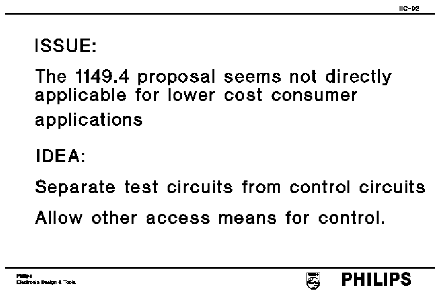
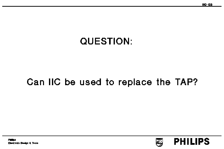
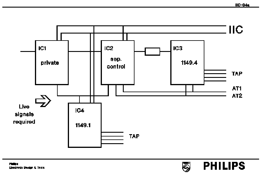
Frans de Jong: IIC - formal response
The following discussion was presented using slides: IIC-01,
IIC-02, IIC-02a,
IIC-03, IIC-04, IIC-04a.
IIC busses are being used for testing at Philips. Philips does have chips
with both 1149.1 and IIC busses on them. Question: Can IIC be used to test
1149.1 chips. Answer: Yes, but it would require extra design efforts and
separate test circuits from control circuits. Normally, IIC usage requires
an IC to be in some sort of functional mode. Also because of this, when
IIC busses are used for testing, together with 1149.1 chips, it often means
having to split up the test into several steps. For this reason it is not
recommended as a general strategy. Keith Baker previously had said it's
possible Philips will use P1149.4, controlled by IIC. This will not happen
as we see it now. When appropriate, P1149.4 will be used as the standard
defines. IIC is used for functional control and sometimes used as an aid
in testing. Mani pointed out that another European company also has chips
with IIC and 1149.1 on them and faces a similar situation.
Frans also showed a photograph of a mixed-signal
tester on a single board SIMM with an ARTEMIS
chip in it. This board is being used in systems. The next step is to put
the entire board on a single chip. Frans also indicated that he could serve
as a liaison between the Working Group and ARTEMIS.
The photograph shows a picture of the prototype
of a mixed-signal test module made by MAZeT GmbH. This is a result of one
of the mixed-signal investigation projects (this one partially funded as
ESPRIT Project 6138).
This module fits in a simm socket and can perform mixed signal tests.
The exact description can be found in the datasheet. The big QFP in the
middle is the actual ARTEMIS chip, containing a 8051-like core, some additional
digital I/O, containing a TAP for controlling Boundary-Scan tests, AT1
and AT2 pins, again to be used as controller and eight analog pins, four
as multipxed inputs and four as outputs. The AT1 and AT2 pins are connected
through a '.4 5-switch' arrangement for performance measurements on this
circuit.
The eprom is temporarily placed in a socket. This eprom contains the
test program for the target board. The chip at the other side is the RAM.
Basically this module performs as a simple test module for board level
self tests. For production tests it might help in combination with an external
tester (the module supports slave mode).
Later versions of the module are planned to be smaller and 'affordable'.
For more information:
Grunert@mazet.de
Krellner@mazet.de
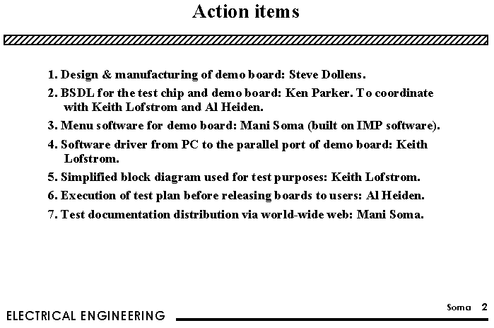
Test chip update: Keith Lofstrom.
Steve Dollens is manufacturing the test chips
and will distribute test chips, demo boards,
and software. Mani is working on menu-driven software for the demo board;
is responsible for test distribution via WWW; and setting up an FTP software
site at the UW web site; and also collecting user feedback. Ken is handling
BSDL. Keith will create a simplified block diagram for test purposes. Al
Heiden will verify test plan before its release. Types of tests are shown
on the viewgraph and handouts
and are self-explanatory. The differential amplifier has a gain of 5, and
operates at 100MHz. Steve will create a few hundred samples. Keith commented
that he wanted to build an imperfect differential amp so we can test it
out using our scheme. A lot more can be learned testing a bad chip than
a good one.
Charles Meyerson's proposal for internal control
cells.
There are 3 options for designing internal
analog test cells:
1. Leave it to designer's discretion. The result is no software assistance.
2. A few simple rules (have enough rules to allow
software to keep track of which nodes are on ATn, give warning for multiple
nodes on ATn; graphical interface to control switches will help). Minimize
overhead allowing flexibility. Result is that software can aid IC test.
3. Restrictive rules -- designers will ignore them, but rules will be uniform.
Page 5 of handout/viewgraph: Ken Parker suggested
this could be a part of boundary-scan register, but Brian said this is
for internal test. The reason for Ken's suggestion is that internal test
cells being a part of the boundary-scan register allows one to control
everything (including the bits in the boundary-scan register). The current
BSDL does not support anything other than EXTEST, BYPASS, and SAMPLE.
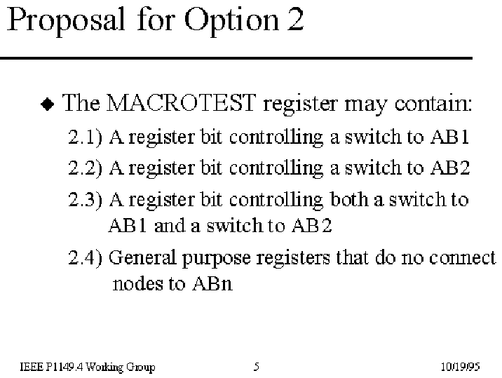
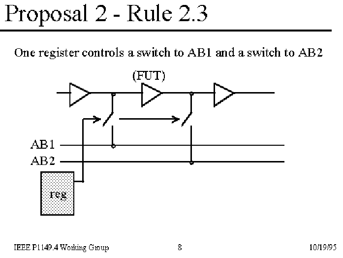
Proposal for Option 2 was discussed initially.
This proposal included the following slides: Rule
2.1, Rule 2.2, and Rule
2.3. After some discussion, Proposal for Option
1 was on the table for voting. Ken wondered if people know what "in
accordance with 1149.1" in viewgraph 3 means.
Lee Whetsel suggested adding "in response to private instruction"
after "operate." But Ken again said we could put this in the
boundary-scan chain and use "disable" to disconnect mission circuit
and it would allow one to load the desired bit patterns in there to do
specific internal testing. Charles said we need to have switches so we
can access internal nodes for internal testing.
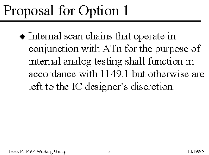
Proposal for Option 1: MOTION: Internal
scan chains that operate in conjunction with ATn for the purpose of internal
analog testing shall function in accordance with 1149.1 but otherwise are
left to the IC designer's discretion. Seconded. Aye: 14. Nay: 1. Abstention:
0. Motion carried.
SUMMARY: For internal analog testing, the Working Group does
not impose restrictions but does require internal testing to be compatible
with 1149.1. Ken suggested maybe we can work the internal testing aspect
into the boundary-scan scheme.
Brian Wilkins' draft:
Brian asked how many people have access to WordPerfect? Almost everybody
has access to Word, and SPAsystem. Adam suggested asking the Working Group
to purchase an Adobe software package for Brian. Brian can then generate
a postscript files and convert them to PDF format for posting on the SPAsystem.
The Working Group currently has about $2000 in reserve. Brian said he can
generate a postscript file and will experiment with this. If the Adobe
distiller works, we can get into a cycle. The Working Group probably would
want to avoid conversion between Word, WordPerfect or any other software
packages.
MOTION: The Working Group authorize Adam to buy software for
Brian. Seconded. Unanimous approval.
16. Cost calculation -- Steve Sunter:
Steve presented a paper which he will give at ITC. The version for ITC
is a lot more general than shown here.
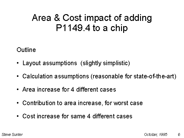
Area and cost impact of adding P1149.4 to chip:
Viewgraph 7. First layout assumptions: Assume
pads side by side. When adding P1149.4, there will be some additional circuitry
at each pin resulting in a net increase of 1 extra pad length in both x
and y directions.
Viewgraph 8. Assumptions list. Assuming we
don't have to go to the next larger-size package. These prices are reasonable.
The idea behind all this work is so that we can convert area to cost.
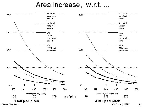
Viewgragh 9. The most cost will be in adding
1149.1 on chips. Next is "adding 1149.1, but die not pin limited."
Third is the case where we already have 1149.1 and only want to add the
2 little extra pins.
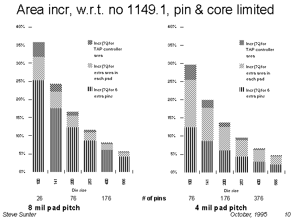
Viewgraph 10. Focusing on just the top curve
of viewgraph 9: A small increase in area for
TAP controller. But the big killer is adding extra pins. Steve Dollens
interjected, saying in some cases that may be a blessing.
Viewgraph 11. Looking at cost increase. When
we get to the large die sizes, the cost goes up (see graphs). It is most
pronounced for the extreme case of no 1149.1 pins. Above half-inch, the
cost escalates. This is why high volume, complex chips are fabbed in the
200-400 mil range.
SUMMARY: The main contributor to cost is adding extra pins. An
increase in area corresponds to an increase in cost.
Balloting schedule.
On handout, change "vendors" to "pushers,"
and "system designers" to "users." Also add "6.
others".
Adam noted that there have been drop-outs as well as newcomers.
Time -1: Develop ballot list, prep balloters.
Time 0: Send out draft for ballot (to all 257 on the list?)
+3 months: Receive votes.
+3 months: Respond to comments/negative votes and re-send ballot.
+3 months: Results go to IEEE before next board meeting.
+2 months: Final standard.
Mani suggested perhaps set time 0 to 5/96. We need to set a goal in
order to make the projected milestones. Or maybe we still need to know
what 1149.1's position is. Still we need to set a target date. Some in
the Working Group don't believe in setting a date. Question posed to Brian
is: Assume 1149.1 somehow could make it go faster, then can we get a draft
to vote on in May? Lee said that 1149.1 is a reasonable group and should
vote on this soon. Adam said we need to have something to review before
sending draft out.
1149.n updates:
No one really knew what was going on in P1149.2 except that the P1149.2
Working Group adopted the TAP.
1149.5 was approved by IEEE in July, 1995. Document is now available
from IEEE. 1149.5 also accepted by VME64 bus. There are 2 papers about
1149.5 at ITC.
Next meeting:
Terry Junge has volunteered for SEAGATE to sponsor the next Working
Group meeting in February, 1996. The format will be split-date. Need to
decide on the day (Thursday-Friday?). In terms of publicity, do we want
to advertise at ISSCC next year? We will have no exposure at ISSCC. Keith
doesn't have silicon so he will have no paper at ISSCC. Anybody can get
in CICC. Debate over the meeting dates ensued. Finally, it was decided
to vote on the 2/96 Working Group meeting dates over e-mail.
Before adjourning, the subgroup on 1149.1/P1149.4 set up a date and
time to meet: After the Plenary Session in the back of the hall.
MOTION: Adjourn meeting. Seconded. Approved.