EXPERIMENTS WITH IEEE 1149.4 KLIC TEST CHIP
A Case Study
Marina Santo Zarnik (Hipot Hyb, Sentjernej)
marina.santo@ijs.si
Franc Novak, Uros Kac, Srecko Macek (Jozef Stefan Institute, Ljubljana)
franc.novak@ijs.si
ABSTRACT
The paper presents some results of the experiments with IEEE 1149.4 KLIC Test Chip in the area of active RC filters implemented in thick-film hybrid technology. The influence of analog boundary modules (ABMs) on circuit performance is analysed in the case study of active RC notch filter.
INTRODUCTION
In this paper we present some results of the experiments with IEEE 1149.4 KLIC Test Chip in the area of active RC filters implemented in thick-film hybrid technology. The thick-film hybrid process is a technology between the monolithic integrated and printed circuit technologies. It integrates the conductive and insulating layers with thick-film resistors on a ceramic substrate. Discrete elements (capacitors, diodes, transistors, integrated circuits, etc.) are soldered, bonded or glued onto the substrate.
An advantage of active RC filters implemented in thick-film hybrid technology is the ability of active adjusting the characteristics (frequencies of poles and zeros, quality factor) by laser trimming of selected resistors. The required performance of such circuits is often specified within narrow tolerance ranges. The goal of our case study was to analyse the influence of IEEE 1149.4 ABMs on the circuit performance. For a rough estimation we first modeled the ABM module by a simple RC circuit and simulated the operation of the selected hybrid circuit with and without ABM modules. Next, real ABM modules were inserted and the circuit performance was analysed.
SELECTED CIRCUIT
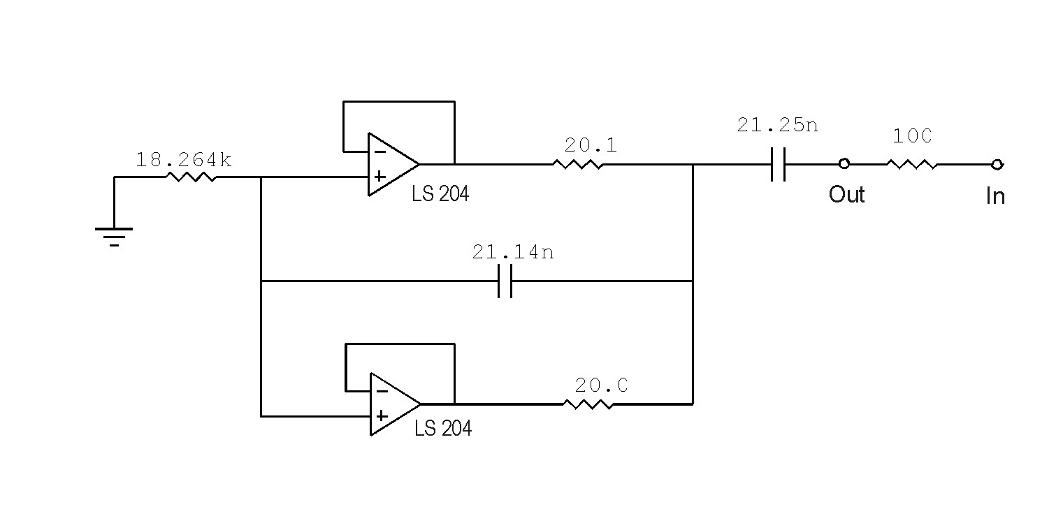
For the case study we have chosen the active RC notch filter (as a part of a thick-film hybrid circuit for a telecommunication application). The circuit under consideration is shown in the next figure. (The values of its components have been measured after adjusting the filter characteristics.)
Figure 1
WLOG we consider the simplified notch filter shown in Figure 2. In order to analyse the impact of circuit parameters on its performance we first express the transfer function .

Figure 2
Assuming ideal op-amp, the transfer function is given by:
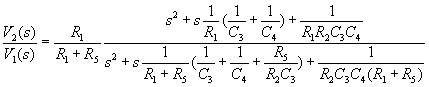
The frequencies of pole and zero, and their qualities are given by:

![]()
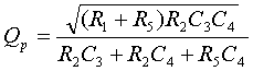
The above expressions describe how individual circuit elements determine the frequency of pole and zero and their qualities. The expressions also apply to the circuit in Figure 1 (assuming the value of resistor R2 = 20W ú ú 20.1W ) and they are used in the first approximation of the circuit design.
Considering non-ideal op-amp, pole and zero positions move to lower frequencies as shown in the simulation in Figure 3.
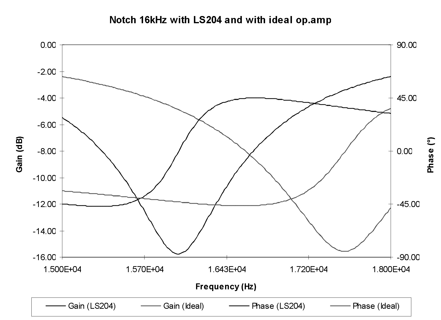
Figure 3
In practice, the impact of non-ideal op-amp is considered in the early design phase and finally compensated by trimming the resistor(s) in the production process. The introduced ABMs have additional impact on filter characteristics. The question is, how much do they actually influence circuit performance, and if it is possible to compensate their impact in practice. In our case we inserted ABMs in the circuit as shown in Figure 4.
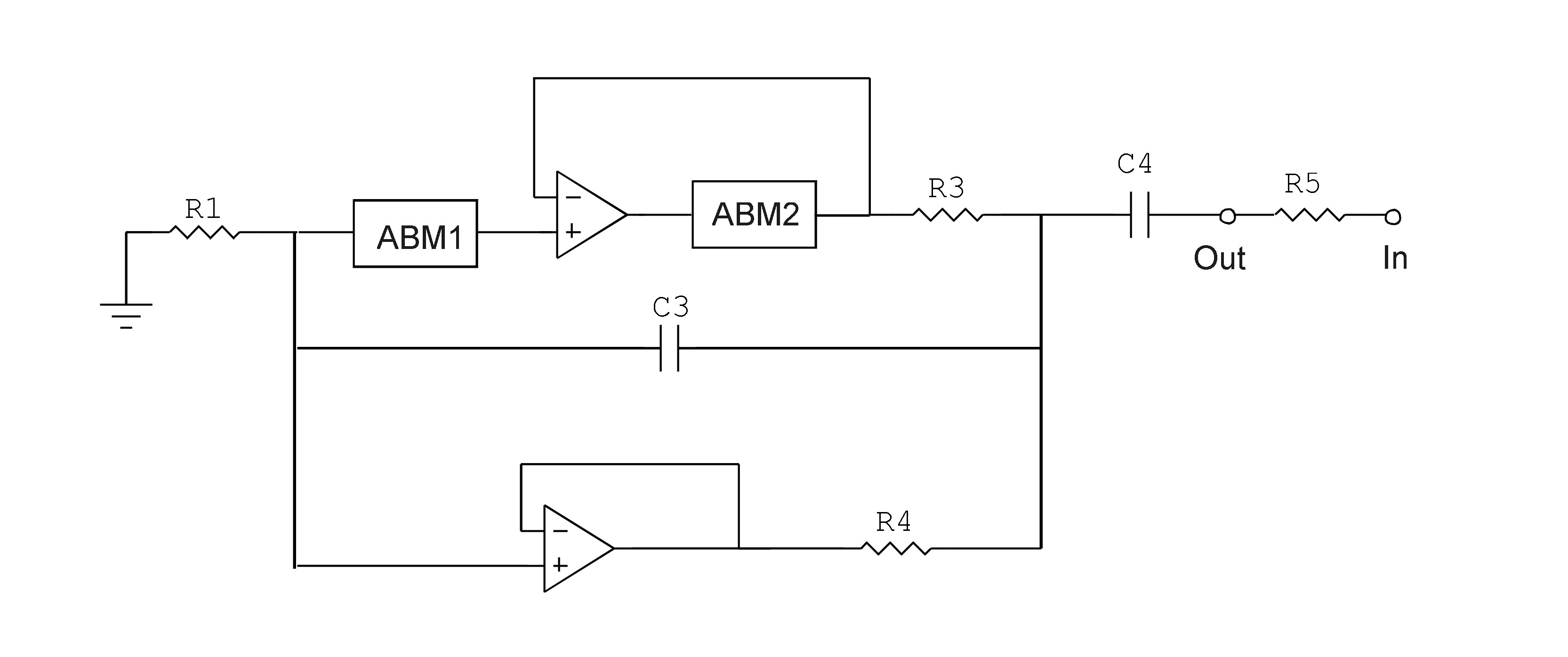
Figure 4
For a rough estimation we modeled the ABM module by a simple RC circuit (Figure 5) and simulated the operation of the filter circuit with and without ABM modules.
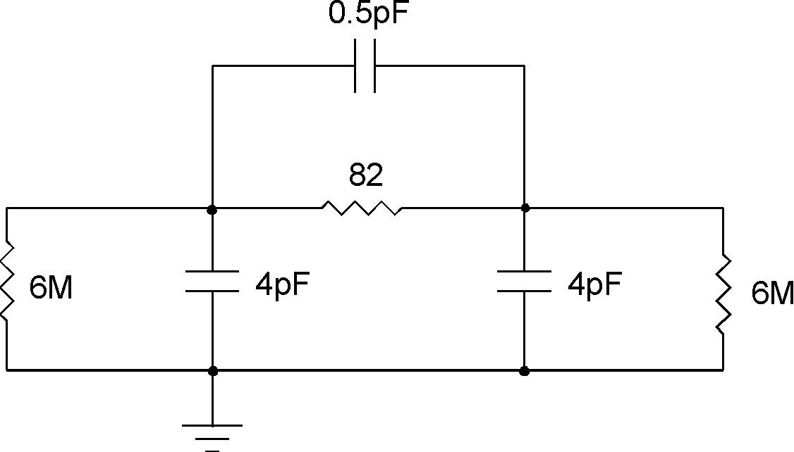
Figure 5
As expected, simulations have shown that the inserted ABM modules affect circuit operation. In the next step, real circuit operation was measured. Comparing the measurement results with the simulations we found that the above model can be used in the first approximation.
MEASUREMENT RESULTS
:Measured amplitude and phase characteristics of the circuit in Figure 1 (without ABMs) is shown in Figure 6.
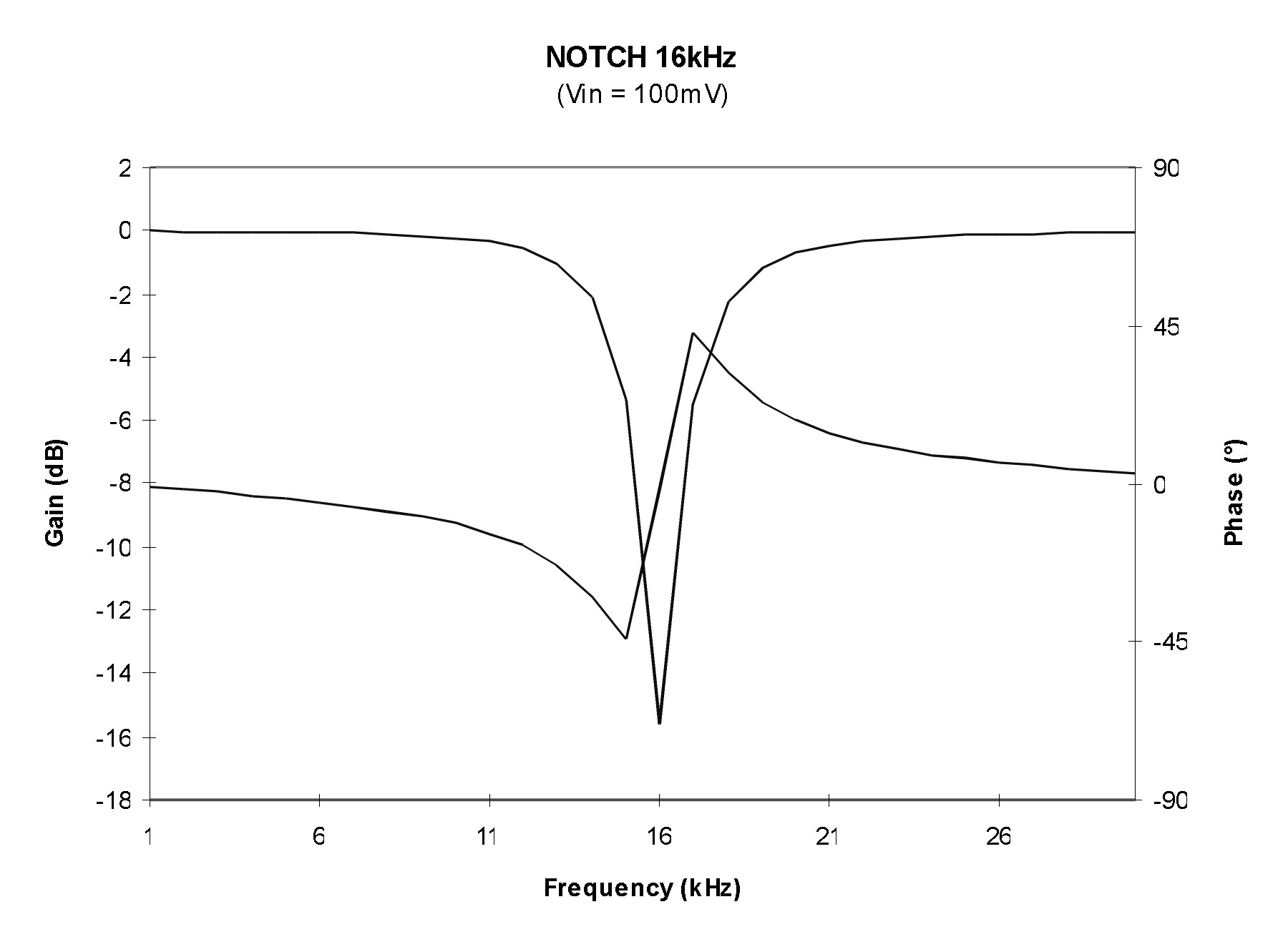
Figure 6
Since the characteristics depend on the amplitude of the input signal, we made measurements at two different input signals (Vin = 20 mV and 100 mV). The normal operation is shown in Figure 7.
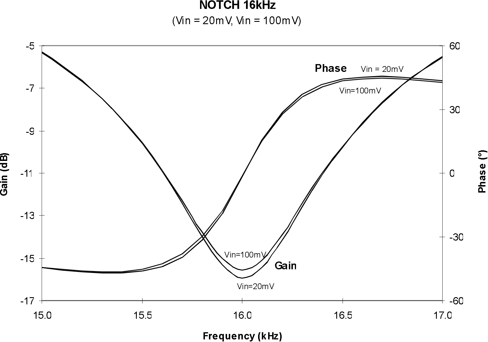
Figure 7
Next we have inserted ABM1 (BC0) at the non-inverting op-amp input as shown in Figure 4. The BCO test boundary cell was wired between the printed metal pad on the hybrid substrate and the op-amp pin. The wire length was about 1.5 cm. The measured characteristics are shown in Figure 8 and 9.
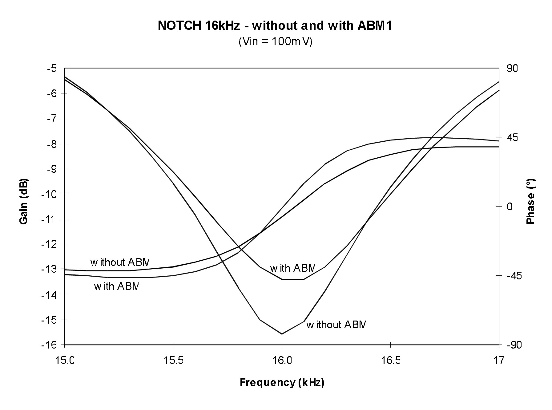
Figure 8
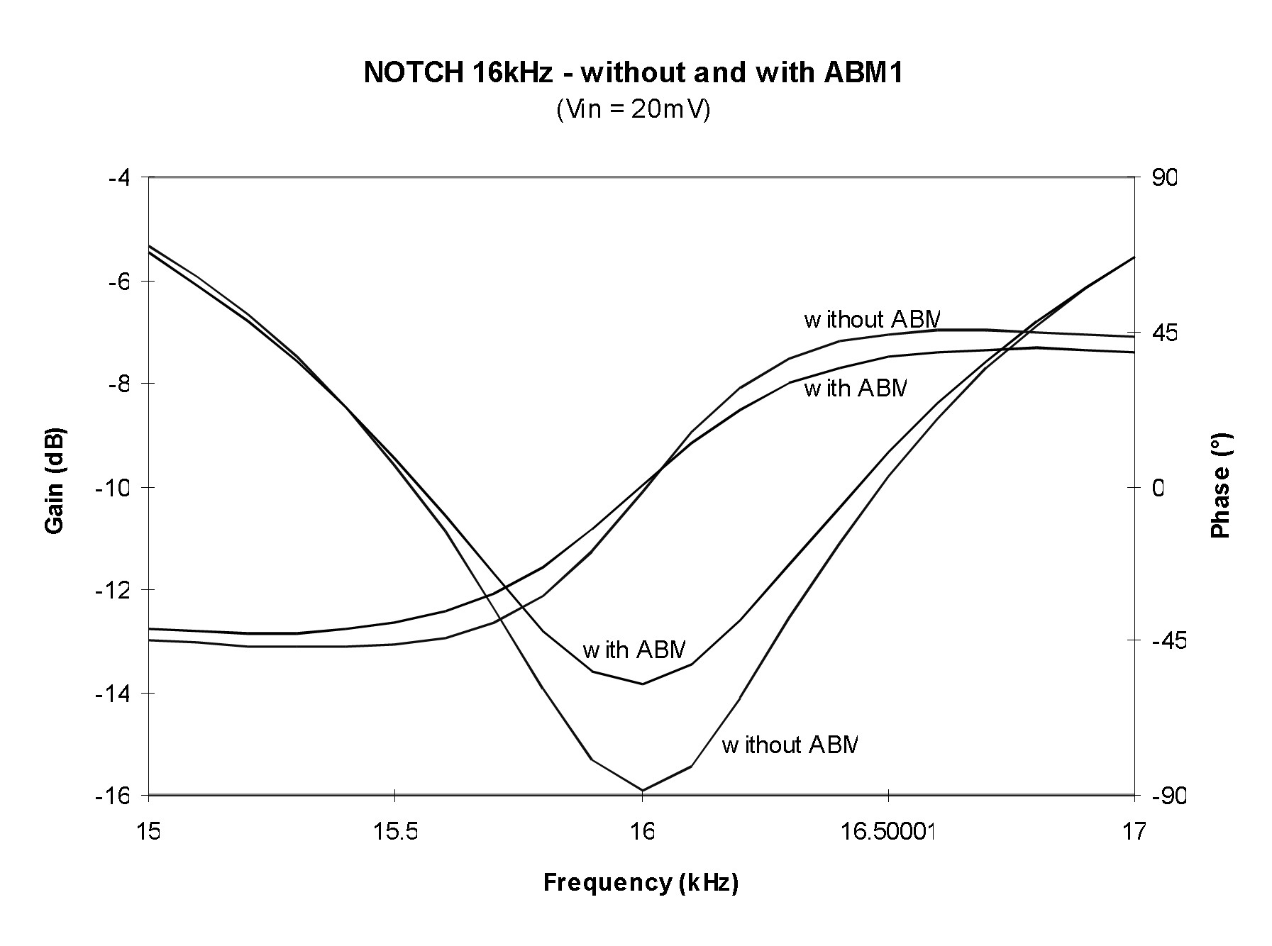
Figure 9
Measurement results in the case of inserted ABM2 (BC0) are shown in Figures 10 and 11.

Figure 10

Figure 11
Finally, both ABM1 and ABM2 were inserted and the measured results are given in Figure 12 and 13.

Figure 12
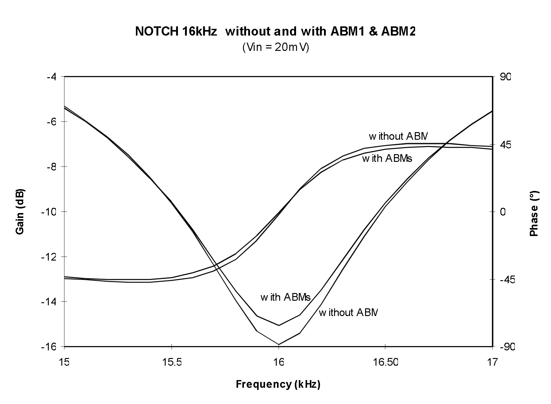
Figure 13
COMMENTS
Inserted ABM1
Measurements indicate that the central frequency f0 shifts towards higher frequencies and the gain at f0 increases when ABM1 is inserted . In the case presented in Figure 8, for the input signal Vin = 100 mV, the frequency shift of f0 is 53 Hz (0.33%), and the gain is increased for 2.12 dB. At the lower input signal Vin = 20 mV, shown in Figure 9, the frequency shift is a little smaller (10 Hz or 0.06%), and the gain at f0 changes for 2.37 dB. The changes are due to the capacitive influence of the inserted ABM1, while the serial resistance of the ABM1 module can be neglected.
Inserted ABM2
Measurements indicate that the central frequency f0 slightly shifts towards higher frequencies and the gain at f0 decreases. In the case presented in Figure 10, for the input signal Vin = 100 mV, the frequency shift of f0 is 12 Hz (0.07%), and the gain is decreased for 1.95 dB. At the lower input signal, shown in Figure 11, the frequency shift is 10 Hz (0.06%), and the gain is decreased for 2.37 dB. The changes are due to the on-resistance of the ABM2, while its capacitive effect can be neglected.
Inserted ABM1 and ABM2
As shown in Figures 12 and 13, the change of circuit characteristic is smaller than in the cases when only ABM1 or ABM2 is employed. This is due to the fact that the impact of ABM1 and ABM2 on the filter quality partially compensate. In the above case, the quality has decreased for less than 3%.
TEMPERATURE MEASUREMENTS
As known in practice, RON of MOS switches depend on temperature changes. In our case, filter characteristics (with and without inserted ABMs) were measured at 0, 25 and 750 C. As expected, the notch frequency moves toward lower values when temperature increases. However, as shown in Figures 14 and 15, the change due to the inserted ABMs (in our case) is not significant.

Figure 14
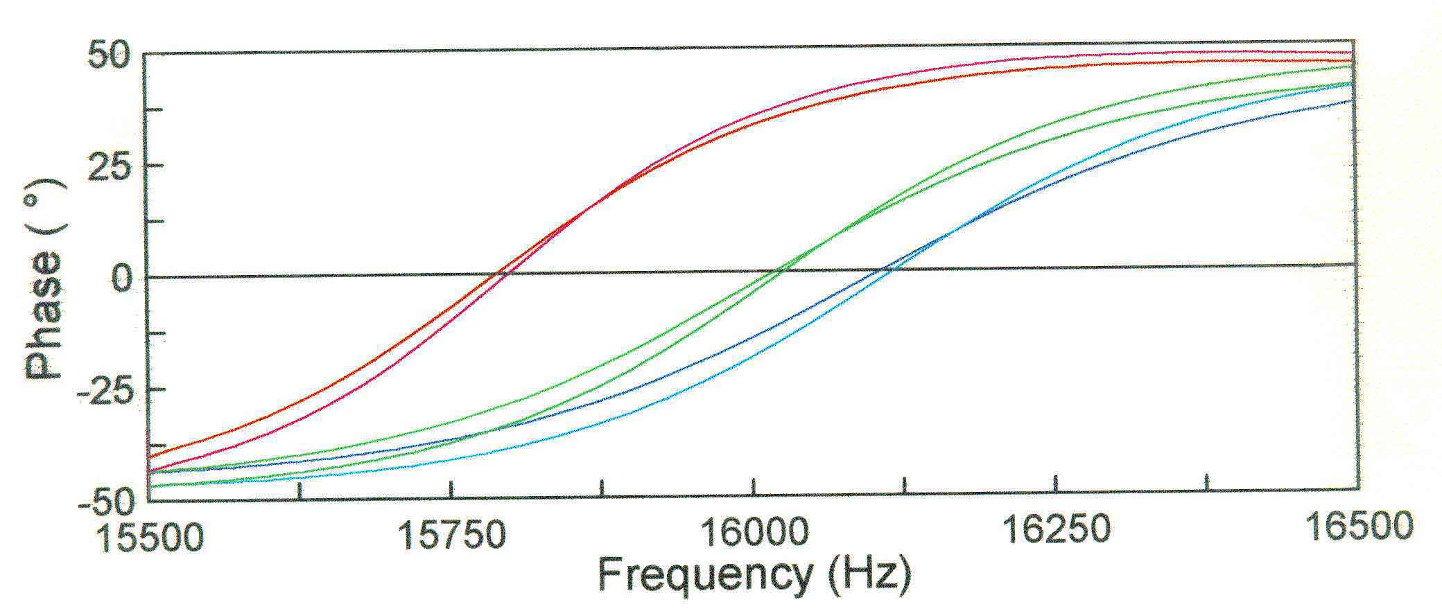
Figure 15
CONCLUSIONS
In our case, the resulting changes of the central frequency f0 are not critical since they can be easily adjusted. More efforts would be needed to achieve the required quality in the case of high performance circuits (narrow tolerance ranges). This is likely to require adjustment of more than one circuit component which is not suitable for the production process. In order to avoid this, the impact of ABMs should be considered early in the circuit design.
REFERENCES