Figure 1
Hello Steve, Brian, Adam and Dot-4,
I'm trying to get to an action item, the structure of the ATn-to-ABn switching, as well as the "final" ABM description.
Un-attached to this document are 4 hand drawn figures. I'll ask Adam to post this document and the figures on the Web. The figures help see what I'm talking about and the MEI drawings are a good reference too.
If you look at the MEI drawings (MEI document from ITC) in Figures 5, 6 and 8 you will notice that none of these are qualified by the current effective instruction, meaning that even during BYPASS, switches can be closed and affect pins and busses. This is an oversight dating back to our 1993 ITC paper.
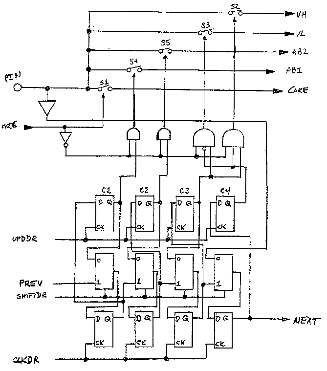
Let me address MEI Figure 8 first, which is the general ABM.
MEI labeled the 4 latch states used to derive switch controls C1, C2, C3 and C4. I'll retain this convention as well as the switch labeling S1 - S5.
MEI shows a "Mode" line. When Mode=1, the circuit is in "mission" mode, according to Table 7 (page 13). This is only really true when C1-C4=0000 which opens switches S2-S4. The mode line itself is used to control S1 (core disconnect). The Table then lists a bunch of "Extest" functions when Mode=0.
Now, we want to have as mandatory, the simplest possible set of rules that will also yield the cheapest and easiest implementations. Here goes! (I will use ASCII equations; a trailing '-' indicates inversion.)
Mandatory Instructions:
BYPASS (Mode=1)
SAMPLE/PRELOAD (Mode=1)
EXTEST (Mode=0)
S1 = Mode
S2 = C3 * C4 * Mode-
S3 = C3 * C4- * Mode-
S4 = C1 * Mode-
S5 = C2 * Mode-
These equations state that only in Extest do the BReg bits have the ability to close switches. Sample/Preload can be used to set up an initial state in these latches. Also during Sample/Preload, the digitized value of the pin state is captured in C4 flip-flop (not latch). During BYPASS, the state of the BReg is completely isolated from the pin.
When Extest is in effect, we have the following table of possible actions upon a pin governed by states C1-C4. IN ALL CASES, S1 is open isolating the pin from the core:
| C1-C4 | S2-S5 | Description | Notes |
|---|---|---|---|
| 0000 | oooo | Pin completely isolated from core, ABn, VH/VL (Dot-1 Z) | 1 |
| 0001 | oooo | Pin completely isolated from core, ABn, VH/VL (Dot-1 Z) | 1 |
| 0010 | oCoo | Pin connected to VL (Dot-1 drive low) | 2 |
| 0011 | Cooo | Pin connected to VH (Dot-1 drive high) | 2 |
| 0100 | oooC | Pin connected to AB2 (analog measure) | 3 |
| 0101 | oooC | Pin connected to AB2 (analog measure) | 3 |
| 0110 | oCoC | Pin connected to AB2 and VL (ref low and measure) | 4 |
| 0111 | CooC | Pin connected to AB2 and VH (ref high and measure) | 4 |
| 1000 | ooCo | Pin connected to AB1 (analog stim) | 5 |
| 1001 | ooCo | Pin connected to AB1 (analog stim) | 5 |
| 1010 | oCCo | Pin connected to AB1 and VL (ref low and stim) | 6 |
| 1011 | oCoC | Pin connected to AB1 and VH (ref high and stim) | 6 |
| 1100 | ooCC | Pin connected to AB1 and AB2 (stim and measure) | 7 |
| 1101 | ooCC | Pin connected to AB1 and AB2 (stim and measure) | 7 |
| 1110 | oCCC | Pin connected to AB1, AB2 and VL (ref low, stim, measure) | 6 |
| 1111 | CoCC | Pin connected to AB1, AB2 and VH (ref high, stim, measure) | 6 |
Notes:
1) Emulate Dot-1 High-Z state, monitor pin
2) Dot-1 drive data (self monitoring), may use full current output driver
3) Used for metrology and "analog sample"
4) Used for metrology (VH/VL must be reference quality levels)
5) Used for metrology and "analog functional test"
6) May be used to characterize/test switches, or measure if AB1 can sense
7) Used for metrology and "analog functional test"
In the above table (states 0-15) we see states 0-3 used for Dot-1 emulation with the option for using powerful drive levels rather than wimpy VH/VL switching. In essence this is selected by C1C2=00. For Dot-1 software, flip-flops C3C4 are "standard" 1149.1 control cell and data cell, with the self-monitor capability. Flip-flops C1C2 are the Dot-4 addition, unused and set to 00 during any Dot-1 activity. Dot-4 software will use C1-C4 for algorithmic metrology, and special uses (like switch characterizatio) can be supported as well.
A word about what flip-flops C1-C4 capture: FF C4 is mandated to capture the digitized pin state. The MEI drawings do not show what C1-C3 capture. I urge us to consider a recommendation that these FFs capture something useful that aids in the testability of the ABM itself. For example, if each FF of C1-C3 captured the output of its respective latches, that gives us digital testability of thier FF/Latch circuitry. Without this, we have to set up analog experiments using ABn and VH/VL to test the FF/Latch circuitry. Perhaps we should flat-out mandate this testability!
The shift order of the FFs in an ABM is arbitrary and may even be mixed with other cells. By NAMING the FFs, we can (in BSDL) correlate the ABM resources to a pin. Thus we need names for them, beyond C1-C4.
Optional Instructions:
HIGHZ (Mode=1)
CLAMP (Mode=0)
IDCODE (Mode=1)
USERCODE (Mode=1)
These instructions behave the same as Dot-1; there must be an indication from the instruction decoder that HIGHZ/CLAMP are being decoded. I'll assume signals named Highz and Clamp. Then:
S1 = Mode * Highz-
S2 = C3 * C4 * Mode-
S3 = C3 * C4- * Mode-
S4 = C1 * Mode- * Clamp-
S5 = C2 * Mode- * Clamp-
Brian, I think we can convert these equations into generic rules, like this for S1:
Rules:
a) A switching function S1 shall be used to isolate (either directly or functionally) a pin from the core circuitry.
b) Switching function S1 shall be closed (connecting the pin to the core circuitry) whenever the instruction register is decoding BYPASS, SAMPLE/PRELOAD, IDCODE or USERCODE instructions.
c) Switching function S1 shall be open (isolating the pin from the core circuitry) whenever the instruction register is decoding EXTEST CLAMP or HIGHZ instructions.
(Some discussion of "connect", "isolate" and "directly or functionally" will be needed elsewhere.)
ATn Port Switching
In the MEI implementation, we have the ability to treat ATn pins as analog ports with indepedent controls, and to do Dot-1 interconnect testing on the ATn pins. (See page 9 of MEI document.)
When either or both of ATn are NOT CONNECTED to their respective ABn buses, a DC voltage is connected to ABn to stabilize ABn to suppress leakage and noise. This voltage is selected by the designer for best suppression characteristics. (Note that in a given IC during a test, only one bus may need to be active rather than both.) In figures 5 and 6, notice that the DC switches (E7, E8) are controlled by the complement of the control for connecting ATn to ABn (E5, E6). Thus, whenever ABn are disconnected, they are automatically connected to the DC voltage.
In the MEI chip, it is possible to connect AB1 to AB2 (switch E9). Given the ability to do Dot-1 interconnect test on the ATn port pins, I'm not sure the E9 switch is needed for anything any more (Steve??). We had thought it would be needed for infrastructure test. I'll leave it in for now, but removing it would eliminate a shift stage in the AT1 control. Removing it would also eliminate the question of "what kind (current or voltage) must this switch be?"
The MEI chip doesn't show Mode at all as a control for any of the switches. I will add it, but notice that the ATn-to-ABn switches are controlled by BReg cells as well as a Mode signal. This allows independent activation.
Below is a table for the 4 bits K1-K3-K5-K7 controlling the switches E1-E3-E5-E7-E9 shown in figure 5 of MEI document (page 10). IN ALL CASES, Mode=0:
| K1-K7 | E1-E9 | Description |
|---|---|---|
| 0000 | ooCoo | AT1 completely isolated from AB1, AB1 connected to DC |
| 0001 | ooCoo | AT1 completely isolated from AB1, AB1 connected to DC |
| 0010 | oCCoo | AT1 connected to VL (Dot-1 drive low), AB1 to DC |
| 0011 | CoCoo | AT1 connected to VH (Dot-1 drive high), AB1 to DC |
| 0100 | ooooC | AT1 connected to AB1 |
| 0101 | ooooC | AT1 connected to AB1 |
| 0110 | oCooC | AT1 connected to AB1 and VL |
| 0111 | CoooC | AT1 connected to AB1 and VH |
| 1000 | ooCCo | AT1 isolated from AB1, AB1 connected to DC and AB2 |
| 1001 | ooCCo | AT1 isolated from AB1, AB1 connected to DC and AB2 |
| 1010 | oCCCo | AT1 isolated from AB1, connected to VL; AB1, AB2, DC connected |
| 1011 | oCCoC | AT1 isolated from AB1, connected to VH; AB1, AB2, DC connected |
| 1100 | oooCC | AT1 connected to AB1 and AB2 |
| 1101 | oooCC | AT1 connected to AB1 and AB2 |
| 1110 | oCoCC | AT1 connected to AB1, AB2 and VL |
| 1111 | CooCC | AT1 connected to AB1, AB2 and VH |
Again, FF C1 and switch E9 which connect AB1 to AB2 seems pretty useless.
Equations for E1, E3, E5, E7, E9: (Note, definition of Mode given above)
E1 = K5 * K7 * Mode-
E3 = K5 * K7- * Mode-
E5 = K3 * Mode-
E7 = E5- = (K3 * Mode-)-
E9 = K1 * Mode-

Now let's examine the AT2 port. This port is controlled similarly to the AT1 port, except it doesn't have the 4th FF to connect AB1 to AB2 since that is in the AT1 port (again, do we need it??).
Again, I'll use the MEI document (page 11) as a starting point. Below is a table for K2-K4-K6 controlling switches E2-E4-E6-E8. In all cases, Mode=0:
| K2-K6 | E2-E8 | Description |
|---|---|---|
| 000 | oooC | AT2 completely isolated from AB2, AB2 connected to DC |
| 001 | oooC | AT2 completely isolated from AB2, AB2 connected to DC |
| 010 | oCoC | AT2 connected to VL (Dot-1 drive low), AB2 to DC |
| 011 | CooC | AT2 connected to VH (Dot-1 drive high), AB2 to DC |
| 100 | ooCo | AT2 connected to AB2 |
| 101 | ooCo | AT2 connected to AB2 |
| 110 | oCCo | AT2 connected to AB2 and VL |
| 111 | Cooo | AT2 connected to AB2 and VH |

Equations for E2-E4-E6-E8:
E2 = K4 * K6 * Mode-
E4 = K4 * K6- * Mode-
E6 = K2 * Mode-
E8 = E6- = (K2 * Mode-)-
Discussion: For both ATn ports, there is the ability to connect the port pin to the internal ABn bus AND to a VH or VL. Is this of any use? If not, and if we don't need to connect AB1 to AB2, then we can reduce both ATn ports to identical structures that contain only 2 BReg cells. Here is an example of how this would look.
First, define switches just like in MEI figure 6 (page 11), but have only two BReg cells called X and Y. Then the operation table would be:
| XY | E2-E8 | Description |
|---|---|---|
| 00 | oooC | ATn completely isolated from ABn, ABn connected to DC |
| 01 | ooCo | ATn connected to ABn |
| 10 | oCoC | ATn connected to VL (Dot-1 drive low), ABn to DC |
| 11 | CooC | ATn connected to VH (Dot-1 drive high), ABn to DC |
And the equations would be:
E2 = X * Y * Mode-
E4 = X * Y- * Mode-
E6 = X- * Y * Mode-
E8 = E6- = (X- * Y * Mode-)-
This structure is simple using only 2 BReg cells, and uniform so that the structure of both ATn ports is identical.
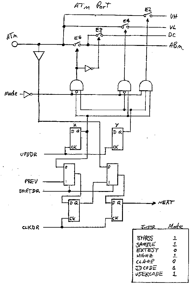
There is a small drawback. Software has to assure that when doing Dot-1 testing (when X is a Dot-1 control cell and Y is a Dot-1 data cell), a tri-stated ATn port should have its data cell set to zero (normally it is a don't care what this cell is) to isolate the associated ABn from the effects of the Dot-1 test. This can be handled by setting the "safe" bit in the BSDL description for the data cell of the port to "0". Properly implemented software should then handle this case automatically.
Laced through this discussion are several questions. Please take a few minutes to consider them. I feel inclined to propose that the attached Figure 1 be representative of a basic ABM and that the attached Figure 4 be the design of both ATn ports. If we can agree to this, then I can help Brian write implementation-free rules.
Regards,
-ken parker-