for
March 4, 1997
| Time | Topic | Responsibility |
|---|---|---|
| 8:00am | Breakfast - Thank you Motorola | |
| 8:30am | Arrival and Introductions | Adam Cron |
| 8:35am | Approval of October, 1996 Minutes | Adam Cron |
| 8:40am | ITC Invitation | Adam Cron |
| 8:45am | Implementation Tolerances | John McDermid Steve Sunter |
| 10:00am | Break - Thank you Motorola | |
| 10:45pm | Switch Leakage Currents | Kozo Nuriya |
| 11:15am | ABM Capabilities | Steve Sunter John McDermid |
| 12:15pm | Lunch - Thank you Motorola | |
| 1:00pm | Control Cells - One or Two References | Steve Sunter |
| 1:45pm | INTEST | Lee Whetsel Keith Lofstrom |
| 2:15pm | Mixed-Signal
VSIA (Virtual Socket Interface Alliance) Working Group |
Steve Sunter |
| 3:00pm | TBIC Requirements | Ken Parker |
| 3:15pm | Draft Review | Brian Wilkins |
| 3:30pm | Break - Thank you Motorola | |
| 4:00pm | Draft Review - Cont. | Brian Wilkins |
| 5:00pm | Ballot Status | Adam Cron |
| 5:30pm | 1149.1 Review | CJ Clark |
| 5:45pm | Next Meeting | Adam Cron |
| 6:00pm | Adjourn | Adam Cron |
| Working Group Members | 34 |
|---|---|
| Total Subscribers | 374 |
| Total Subscribers on "esd" reflector | 279 |
| Countries Participating | 32 |
| Companies/Universities Participating | ~240 |
| Funds Available | ~$877 |
| Name | Company Sponsor |
|---|---|
| John Andrews | National Semiconductor |
| Terry Borroz | Teradyne, Inc. |
| Tapan Chakraborty | Lucent |
| C.J. Clark | Intellitech |
| Jim Coleman | Lucent |
| Adam Cron | Motorola |
| Firooz Farhoomand | Matsushita |
| Grady Giles | Motorola |
| Katsuhiro Hirayama | Matsushita |
| Hank (Hiro) Koyama | Matsushita |
| Tom Langford | Symbols Logic |
| Adam Ley | Texas Instruments |
| Keith Lofstrom | KLIC |
| John McDermid | Hewlett-Packard |
| Elbert Nhan | Johns Hopkins University |
| Kozo Nuriya | Matsushita |
| Ken Parker | Hewlett-Packard |
| Mike Ricchetti | Sunrise Test Systems |
| Takeshi Shimamoto | Matsushita |
| Mani Soma | University of Washington |
| Steve Sunter | LogicVision |
| Tony Suto | GenRad |
| Lee Whetsel | Texas Instruments |
| Brian Wilkins | Southampton University |
| Name | Company |
|---|---|
| Bill Coombe | Medtronic |
| Dan Dandapani | University of Colorado |
| Terry Junge | Seagate International |
| Henry Ng | Analog Devices |
| Michel Parot | Thomson-CSF |
| Bob Smith | Hewlett-Packard |
Adam Cron announced he has dropped 2 names from the WG since they have
not been attending meetings and keeping abreast of the developments in
the WG. He also announced Tony Suto is now officially a WG member, having
fulfilled the attendance requirement and contributing to discussions in
WG meetings. The WG now has 34 members.
Approval
of October, 1996 Minutes
Adam received a motioned to approve the October, 1996 minutes. Seconded.
Unanimous approval.
Refer to Viewgraph VG1. Ben Bennetts, this year's Program Chair
for ITC, is organizing a special session at ITC focusing on the 1149.x
standards. He specifically asked Gordon Robinson to be the session chair
and Colin Maunder, Harry Hulvershorn, and Adam Cron to be the presenters
for the IEEE 1149.1, 1149.5, and P1149.4 papers, respectively. Gordon has
been given the option to deliver a fourth paper on the "potential
synergy of the three Standards in the area of system and field service
with reference to case studies wherever possible". The deadline for
regular paper submission is February 21. However, only an abstract for
each paper is required by February 28. By March 7, papers should be of
sufficient length and material so they can be refereed. The final version
will not be due until July 25. The papers will be included in the Proceedings
and possibly in a special issue of IEEE Design & Test of Computers
or JETTA.
With regard to the developments just described, Adam formally asked
for help from the WG. He said he will give a technical overview of P1149.4
and will need help in ESD. Adam will use Matsushita's 43 ohms as a highlight
and also report on test chips which Adam sent to requesting companies.
Therefore, he will need to supply test data for the test chips (or at least
a promise to produce data) and submit by this Friday. Also included will
be various graphs, Keith Lofstrom's test chip data, Mani Soma's Boeing
test chip linked to an internal test bus. Adam reiterated that he hoped
to get test data from the people that received the Matsushita test chips.
As noted above, a full-text copy of the paper is needed by March 7. Adam
asked how to submit an ITC paper with "no meat" in it and have
it accepted and then add details later. John Andrews commented that with
the credential of being a WG chair such as Adam's, there should not be
a problem to have it accepted. Besides, this paper will be technically
significant and of potential industry-wide value. John cited that when
he was on a review committee, he rejected a lot of sales-pitch type papers.
Steve Sunter said one of the action items from last October's ITC meeting
was determining how to achieve accuracy on currents, voltages, and linearity.
We need to have targets that should be written into the Draft. Steve invited
the WG to comment on his presentation.
Refer to Viewgraph VG3: Measurement Objectives (not rules): For the
range of 10 to 100 kOhms, +/-1% accuracy is proposed at the function pins
only (if the impedance is in the bus, it can be calibrated out). Outside
this range, there is a shoulder region (+/-10%) on either side. It should
be noted that these are somewhat "soft" limits/specifications.
Since CMOS bipolar diodes may be employed, measurement voltages should
not be near 0.7 Volts (i.e., keep measurement amplitudes to within +/-100
mV) that would turn on the diodes. In addition, stimuli should be less
than 200 kHz in frequency. For a 200 kOhm bus or pin capacitance of 25
picofarads, the 3-dB point is about 200 kHz. Steve emphasized that currents
and voltages should not induce signal amplitudes greater than +/-100mV,
responding to Brian Wilkins' question about signal amplitudes. As far
as measurement errors, there should be no single source causing greater
than an overall 25% error for all identified error sources.
TBIC/ABM Current Requirements. AT1-AB1-ABM path: This path should have
the characteristics of +/-100 uA; bus leakage of greater outside the +/-25
uA range shall be documented; gain shall be within +/-0.1% for sine wave
amplitudes within the above limits with DC bias less than the bus leakage.
In other words, any deviation from the rules just described shall be documented.
Clarification: The AT1-AB1-ABM path does not include a path through any
"g" switch, just the AB1 switch (and off chip with this current).
Bus leakages outside the range of +/-25 uA shall be documented. Undocumented
leakages will be assumed to be within the specified range. The limits are
arbitrary. Ken asked if a constant current of 1 mA is fine as long as it
is documented. Steve said yes. Tony Suto said it should be within the linearity
range which in itself is a separate issue. Ken asked about the stability
of the current. Steve said it has to be stable and added that an upper
limit is necessary. Brian said it should be as small as possible but needs
to be a firm limit. John McDermid said the limit should not be too large
since that would limit the measurement dynamic range. Steve said even an
offset current can easily be greater than 25 uA. Mani pointed out that
stability is a function of time and is an important issue. Steve summarized
by saying that we need stability specifications for the bus leakage as
well as for the noise.
The gain of a buffer should be constant to within 0.1%. Again, the measurement
characteristics proposed above should be characterized via the AT1-AB1-AT2
path before measuring components. The gain applies to both AT1-AB1-AT2
and AT1-AB1-ABM paths. Steve reiterated the need of the requirements to
meet the measurement objectives. Tony asked about 10 Ohms, 1% accuracy.
Adam said the bus leakage applies to note a. Steve said these are the only
rules for currents.
Refer to Viewgraph VG4: Proposal for Default Parameters of Noise and
Bandwidth. The proposal is intended to make the proposed specifications
independent of implementations utilizing buffers or transmission gates.
The specifications include the overall effect of both stimulus and measurement
and the requirement that any deviation from these limits will have to be
documented. In Viewgraph VG5, every pin should pass this test but the test
is not mandated (1 kOhm resistor hanging from the pin to ground). Viewgraph
VG6 shows recommendations made for both noise and bandwidth. Mani asked
what about 1/f noise for medical and other low-noise, sensitive applications.
At the minimum, the low end of the noise spectrum should checked to see
if it meets the recommended levels, Mani said. John cautioned that the
limits for the bandwidth still need further refinement. The 0.5% limit
may need to be lowered. Mani asked what about shot noise. Shot noise is
present when injecting a current. John replied that should be an engineering
judgment and is adjustable in the noise specifications. Steve asked whether
we should look at a specific frequency and only concern about what happens
at that particular frequency. Referring back to Viewgraph VG5, Steve said
a current of 100 uA through a 10-kOhm transmission gate impedance will
result in a voltage drop of 1 Volt. Between any two pins, therefore, the
impedance should not exceed 10 kOhms including the two switches in between.
The rectangular box hanging from AT2 on the same viewgraph represents a
measurement device. Steve said the 100 mV limit applies to component under
test, not the AT1 pin. Lee Whetsel asked if this is a stand-alone chip
or a board. John replied that this concerns a transmission gate/buffer
in the AT1 path. Brian asked about the function of the switch shown. John
said it is for noise measurement. The sinusoidal source symbol should really
be a current. Tony asked whether we should allow for a larger voltage amplitude
for stimulus. Steve said no since it would result in the diodes being turned
on. The +/-100 mV are firm limits.
More discussion on Viewgraph VG6 (Recommendations). Keith Lofstrom asked
what about phase change. There should be a limit on the phase since an
amplitude can be constant or flat but the phase may be varying from +90
to -90 degrees. The phase change should be small within the bandwidth.
Keith raised the concern that off-chip there will be some loads that will
affect the chip. Hence, off-chip capacitance limits should also be imposed.
Steve said this topic should be an action item with Keith being the lead.
ACTION ITEM: Keith Lofstrom will lead the investigation of the
effects of off-chip loads on measurements and will also examine the phase
change limits.
Steve said a 1-kHz bandwidth across a 100-kOhm impedance will induce
a 100-mV thermal noise. This is fine but the chip itself may not contribute
more than 0.75 uV. The question is whether this thermal noise ceiling is
realistically achievable, asked Keith. An 18-nV per root Hz is considered
"quiet" for a low noise amplifier. Tony said a typical amplifier
will have a noise specification of 10 to 20 nV per root Hz. Steve said
amplifiers have large transistors to keep the noise down. Tony asked given
the specifications as follows: 32 nV per root Hz, 1 khz bandwidth, 10 ohms
impedance, and 0.1% accuracy, what is the typical bandwidth? It depends
on the wait time. Steve said with those numbers, we should be able to meet
the noise specifications (just the thermal noise). Steve asked if there
is any data from the Matsushita chip on noise. The answer is not at the
moment. The one-kOhm impedances being used in the Matsushita chip is the
geometric mean of 10 ohms and 100 kOhms.
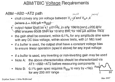
Refer to Viewgraph VG7: ABM/TBIC Voltage Requirements. In the ABM-AB2-AT2
path, there is another reason to constrain the bus leakage to 100 uA (see
hand-sketched drawing on the viewgraph. This example provides an extra
incentive to have a lower swing on the signals. Mani said a 100-uA current
through a 10-kOhm resistance will yield 1 Volt which would then turn on
a bunch of diodes. Therefore, the voltage lower limit should be -100 mV,
and the voltage upper limit should be +100 mV (inconsistency noted in VG7
the second-bullet item). For the stability specifications, it should read
"measured from 0 to 10 kHz". The gain specifications will only
affect signals at a single frequency. The above discussions resulted in
the second-bullet requirement on the viewgraph being deleted altogether.
Also, in the first requirement listed, the delta symbols were changed to
"100 mV".
The CMOS switch impedance should be constrained. Refer to the graph
of Rsw as a function of bias voltage on the same viewgraph. The impedance
change of a CMOS switch with varying bias is evident. The impedance change
of a CMOS switch with a 1-MOhm load at AT2 should therefore be less than
1% to meet the requirements imposed earlier. One requirement is for the
10-kOhm resistor to be very stable. Ken asked if any of these specifications
are attainable. The impedance change vs. bias voltage graph is for a MOS
analog switch model used by Matsushita. For voltage buffers, there is an
offset voltage. In this case, what is permissible? The answer is any offset
can be tolerated as long as it is linear and characterizable. Note that
the above discussion applies to the AT1-AB2-AT2 path whereas the requirements
on VG3 are for a AT1-AB1-AT2 path.
Refer to Viewgraph VG8: Reference Voltage. The reference voltage shall
be a constant voltage between Vss and Vdd. To be consistent with VG7, the
second requirement for noise on this viewgraph was deleted. Ken asked Steve
how to distribute Vl. Steve replied that typically it is the rail. There
is another issue of coupling capacitance. Ken asked whether IR drops on
the metallization in the chip are an issue. Mani said the present Draft
only specifies that Vh and Vl must be supplied. Ken asked whether there
are any new layout rules or specifications with respect to these new rules.
Steve said Vl is pin-specific and that we are not accessing all Vl's simultaneously
at the pins. Every pin may have a totally different Vl. Lee asked if it
is easier to specify a constant Vl throughout the chip (at every pin).
The answer is that a constant universal Vl cannot be specified because
there can be multiple rails used by different chips. John Andrews pointed
out that we have not addressed the "hundreds of milliVolts of noise
in the power supplies". Also, we are only concerned about 1 kHz, but
the clock noise is out of the bandwidth in the mHz range. Ken said we will
have to power condition to run P1149.4 boards. John said it may be possible
to get accurate measurements despite the noise. Ken said we should just
include in the Standard caveats that warn users of potential problems.
John added that averaging the measurements should help. John McDermid and
Brian Wilkins joined the discussion saying internal noises should be suppressed.
Any on-chip noise sources should be minimized and limited (e.g., switch-mode
power supplies). The use of variable-frequency power supplies and other
noisy power supplies should therefore be minimized. John made a final comment
that there are frequency-locking devices that might affect the proposed
measurement bandwidth. The consensus of the WG was for the this topic to
be discussed off-line.
Refer to Viewgraph VG9: Documentation Requirements. Clarifications were
made to the viewgraph contents. Brian pointed out that V=(Vh+Vl)/2 can
have a value of 0, +/-5 V. The "Z" box means it can be more than
just an impedance, e.g., a resistive network. Zp is connected to some node
other than ground. The ground symbol on the load Z is not earth ground.
Mani said we are assuming the chip designers can measure Zs and Zp to the
accuracy required. Ken asked at what frequency the impedances Zs and Zp
are determined. Steve said measurements should be made within the measurement
objectives/guidelines on his earlier viewgraph. Mani asked if we need to
test every pin to get Zs and Zp. The answer is no (it is guaranteed by
design). The impedance for bondwire is typically less than 1mOhm. Ken asked
whether we can assume the effects of Zs and Zp are negligible if we do
not document anything. Steve replied saying systematic errors should be
less than 1%, and random errors should be less than 0.25% since random
errors add in a geometric fashion. Tony then asked about independent sources.
Steve said when disconnected there must be no independent sources in the
system. CJ asked why should limits be imposed; why not just document everything?
If a chip is P1149.4-compliant and if specifications are within limits,
there is no need to document or mention them. Conforming to the specifications
set forth is implied when a chip is labeled Dot-4-compliant. These specifications
are verifiable by the buyers of Dot-4 compliant chips. John Andrews raised
a question about capacitance at 200 MHz, which leads to the next viewgraph.
Refer to Viewgraph VG10: Potential Accuracy Problems. First case: An
undocumented Rs of just 1 Ohm will induce a 10% measurement error at an
input pin in measuring a 10-Ohm impedance. Second case: at an output pin,
an undocumented Rp of 1 MOhm will result in a 10% measurement error when
measuring a 100-kOhm impedance. An example is an amplifier driving an input
pin. It is unrealistic to expect higher precision in either case. In short,
the user will not have to document impedances if they are within limits
but should document them for better accuracy. It is entirely possible to
overdocument parameters. Usually there is an output pin and an input pin
connected to a node. Steve suggested to choose the right one to do measurement
of off-chip loads (i.e., low impedance loads should be measured via an
output pin, and high impedance loads via an input pin). Brian agreed with
the proposal. He wondered if all these limits will ensure meeting the constraints
imposed. Lee Whetsel said P1149.4 is like a mixed signal tester at the
bondpad - off-chip loads can be measured with respect to the bondpad.
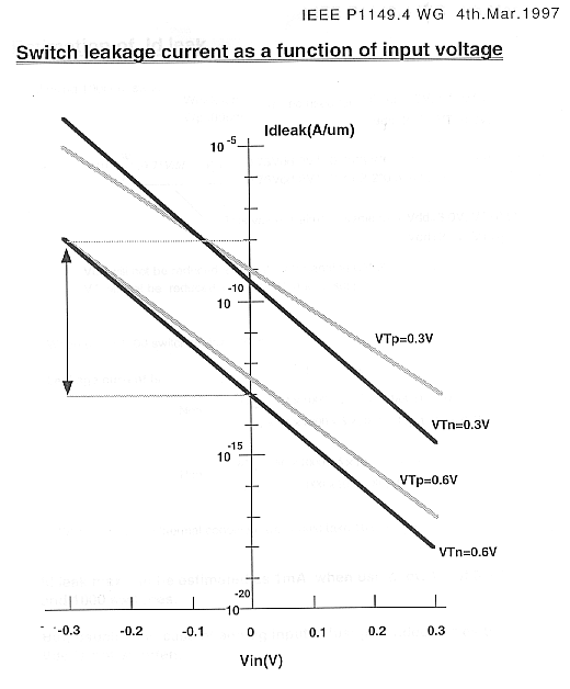
Refer to Viewgraph VG11. Keith Lofstrom asked if the issue of leakage
current to the substrate was addressed. The answer is no. The fact is that
lower voltages will cause a larger leakage current, and these are real
leakages associated with real devices. The leakage model for the switch,
parameters such as theoretical leak current, empirically determined leakage
current for the 0.35-um CMOS switch, and switch-on conductance are given.
Viewgraph VG12 shows the variation of the switch leakage current to changing
input voltage. It should be noted that there is a change in the leakage
current of an n-channel MOS analog switch of approximately five orders
of magnitude over a change of a mere 0.3 V of Vin (Vin=0 to -0.3 V). A
recurring theme is that the lower the voltage the faster the switch operates
but at a price of a larger leakage current.
Refer to Viewgraph VG13: Estimation of Id Leak. Leakage current calculations
were performed using a thousand 100-Ohm switches (both n- and p-channel)
at low voltages. The leakage current was estimated to be 80 uA which when
multiplied by 10 to account for thermal conditions resulted in approximately
1mA. For the n-channel switches, the number is lower. For high-performance
processes, large leakage currents are the price to pay. Steve Sunter will
address the leakage issue later on. These are worst-case calculations.
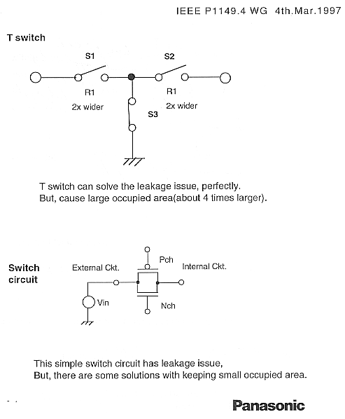
In response to a number of questions from WG members about the MOS analog
switch featured on VG11, Keith proceeded to provide a brief primer on the
T-switch. Viewgraph VG14 shows that the switch diverts leakage currents
on its input pin to ground instead of allowing it to leak into the bus
at its output pin. Whenever switches S1 and S2 are closed, switch S3 must
be open. At the same time, the +/-100-mV window should be observed. Adam
asked about the possibility of employing T-switch for the TBIC. When the
transistor is turned off, only ABMs contribute to the leakage current.
The issue here is that an ABM either can provide reference quality measurements
or, with a change of instruction, provide interconnect testing capability.
Brian added that it would make the table in the Draft much more complicated
if we insisted on having both capabilities. A global signal does not dictate
a reference quality Vh and Vl or the logic version of the voltages. On
the chip, the question is, do we need some pins to have reference quality
Vh and Vl voltages with other pins having just the digital-quality Vh and
Vl. At present, one may switch between them. Ken reminded the WG that 1149.1
pins have more drive while P1149.4 pins with the reference quality levels
might not have enough drive. So far, reference-quality measurement capability
is invoked by the MEASURE instruction while the EXTEST instruction is for
1149.1-type measurements (already motioned in). Adam asked whether we are
going to motion in the table on Page 37 of the Draft. The table contains
both EXTEST and MEASURE instructions for both 1149.1 and P1149.4 measurements.
Adam wanted to know if this dual capability has been agreed on. Brian said
there are no restrictions on the instructions mentioned in the table. Do
we want the high drive capability as an option? If not, the second diagram
has to be modified.
Ken summarized the discussion by saying there are two instructions:
MEASURE and EXTEST. It is possible to globally extend both capabilities
to all pins or locally at each pin specify either capability (selectively
control the individual pin measurement capability). If the latter is chosen,
then the MEASURE instruction is not required. Since both instructions have
the same bit path, if we do not differentiate between the two capabilities,
we would lose the capabilities. If an extra bit is used for differentiating
between the instructions, then both capabilities would be global. There
are some unused states that can be used. Steve and Ken were leaning toward
the status quo.
Lee Whetsel's 3-bus proposal was introduced in 1993 and rejected but
now is being brought back up. This viewgraph illustrates a way to implement
the 3-bus proposal by time-sharing the use of the AT1 and AT2 pins to provide
externally programmable VH, VL, and Vref voltage levels during Dot4 interconnect
test mode, and to provide externally programmable guard (G) voltages levels
during Dot4 measurement mode. Steve said this is assuming every output
converted to the same gain and the reference will be the same globally.
Tony said that the charge time is I / t. John Andrews did not think this
scheme would work since it implies that the clock can be stopped. Keith
said instead of a capacitor, use a flip-flop and a DAC. The DAC can be
small but not necessarily monotonic. Lee said a sample-hold can be used.
Keith said other better ways are possible. Steve asked what about noisy
sources. The prerequisite for this scheme is a very quiet environment in
P1149.4. Steve said this is constraining designers to make it real quiet
and they might not be interested. Noise is everywhere and for higher current
drives, there will be more noise. The driver providing high and low will
drop out of the picture in the reference mode.
Refer to Viewgraph VG16. Some of the noise sources cannot be canceled.
It may not be possible to eliminate the 3SOA noise. So, there are some
disadvantages. Two analog and digital voltages are being time-multiplexed
and will load down the system leading to longer test time. Keith commented
that this scheme might lend itself to more complex applications but might
not work in P1149.4. Ken said RUNTEST idle might be affected because of
glitches produced when switching between the high-drive mode and the reference
voltage mode.
1. Do we allow per-pin control of 1149.1 and P1149.4 measurement modes? Brian said we can. Steve said it has to be compatible and not just a 16-bit machine. To be able to drive logic 1 and still be capable of monitoring voltages and currents at the inputs and outputs is certainly an attractive selling point. Ken suggested to require 1149.1 compatibility while allowing for per-pin control of the measurement mode. Adam said Colin Maunder had suggested sometime ago not to mention bits, instead, think function, and allow the flexibility of specifying any number of bits. Ken was opposed to the idea saying that concept would not be viable. Steve pointed out that there are leftover states that can be used in conjunction with a different decoding scheme. 2. Do we really need two reference voltages for the P1149.4 measurement mode (such as in the Panasonic specifications for the Matsushita test chip)? If only one is needed, then at what level? If only one, should it be per-pin or per-chip? The decision may have to be made taking into account software considerations. Keith asked what the reference level should be. There is always some voltage reference needed in a design that should be specified. A quality reference voltage may not be any of the power supplies. Depending on whether the reference voltage will be per-chip or per-pin, it would be necessary to keep track of the reference voltage in software (if per-pin). Again, the question is "do we really need two separate references?" If only one is needed, it would simplify the number of bits. Steve said we could pick either Vh or Vl to be our reference but we don't know their values. Mani concurred saying we would probably need just a high-quality reference. The need for two references originated from EXTEST requirements. Steve commented that it is not a big deal to add gates. But switches require ESD protection and therefore they could be bulky. Keith said there might be some cases where two references are needed. Brian said we can't extend the capability forever.
Ken Parker initiated a motion: Given that it is possible to solve the
requirements with P1149.4 control cells, we want to mandate:
Discussion ensued. Keith asked "given that" be replaced by
"if". Adam Ley suggested "analog" be replaced by "P1149.4"
for clarity. CJ asked if item 1 above is not satisfied whether it means
we can't have items 2 and 3. Steve said the table on Page 37 of the Draft
(also the January 17 e-mail) there is one unused state. Adam Ley said the
MEASURE instruction is not in existing software yet. It will work, Ken
said, when an EXTEST instruction is supplemented by a bit telling it what
to do. Steve would like the last clarification (item 3 above) be removed.
There are 4 extra states not in the table on Page 37. There is really no
need for +V (a separate motion is needed to deal with the issue). The consensus
was then to delete item 3 altogether. CJ asked to add "interconnect
algorithms", and delete "software" in item 1. Steve said
all P1149.4 chips must be 1149.1 compatible and the software would need
to be able to support 1149.1 tests. Brian advised not to be too concerned
about the wording at the moment.
The revised motion now reads:
MOTION: If it is possible to solve the requirements with P1149.4 control
cells, we want to mandate:
Seconded. Yea: 17. Nay: 0. Abstention: 0. Unanimous approval.
Keith Lofstrom's motion on reference voltage:
Reference quality for both Vh and Vl is not required for a basic ABM.
The minimum 4-bit ABM will drive a strong Vh, a strong Vl, reference quality
voltage, and high-Z.
Ken seconded. Discussion followed. It was suggested that "for both"
be inserted before "Vh and Vl". Keith said this motion is to
settle on the number of high-quality references. If only one is mandated,
one would tend to choose Vl (instead of Vh). Describing in detail what
this reference should be will be laborious. John said a voltage is not
sufficient but the direction of the current flow needs to be known (e.g.,
a voltage regulator which only regulates its output voltage in one direction).
Adam then asked whether the voltage at a node would indicate the direction
of current flow? Not necessarily. Keith is willing to convert this into
an action item instead of a motion since it appears it might not be possible
to come to a consensus at this meeting due to the level of complexity of
the issue. John also questioned whether we could solve this problem here
and now since we don't really know what a reference should be. A straw
vote conducted indicated it has a chance of passing. Hence, the issue is
tabled for e-mail discussion. The WG has two weeks to think about this
and then the discussion will start. John McDermid was just trying to take
into account nonlinear devices such as a diodes. Adam Ley said it probably
would not matter going with either a sourcing or sinking reference, but
sinking/sourcing reference might not work. Brian said as far as the Draft
is concerned, the design of the ABM would be affected. Steve did not think
one or two references would affect the design of the ABM. Steve said the
space is there for two references but this option has always been there
since Day One; it just has never been decided on what to do with them.
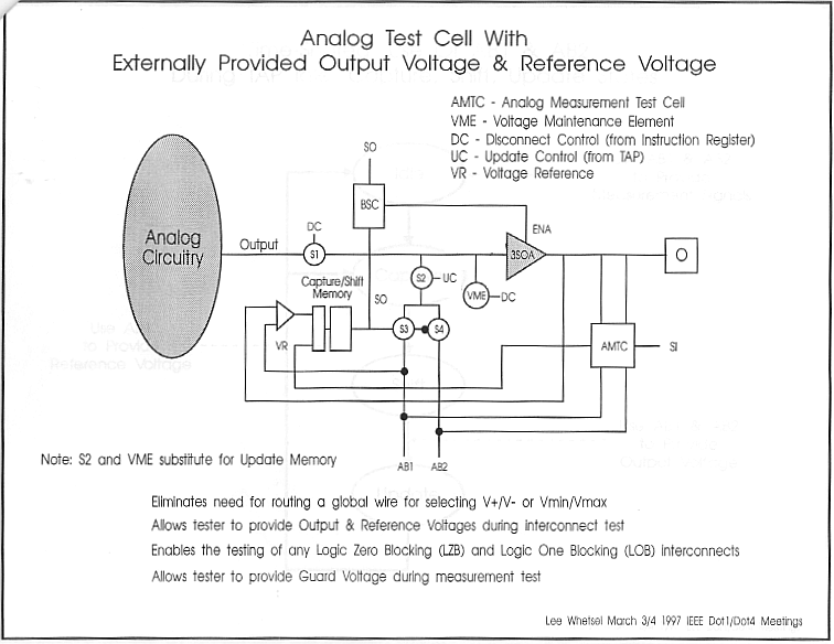
Refer to Viewgraph VG15. Prior to presenting the Dot4 INTEST proposal,
Lee formally rescinded his earlier proposal (VG16 & VG17) regarding time-shared
use of the AT1 and AT2 pins in the interest of moving forward with the
current approach.) Adam Cron asked what to do with multiple analog pins
when an INTEST instruction is scanned in. The analog pins would all have
the same AT1 value. This proposal only says that using an INTEST can test
chips but if specific applications then it would be different. Ken said
this discussion is restricted to only one analog pin but what about multiple
analog pins (we would probably need multiple AT1 values). An example is
an A/D converter with an analog input and a Vref input (an unpleasant scenario).
Lee said if multiple analog inputs cannot be controlled by INTEST, then
it is not INTEST at all (or INTEST in a different sense from 1149.1). Keith
suggested another term for INTEST. When we say INTEST, people think of
1149.1 INTEST. Steve asked what controls the S switch in VG15 (not AB1).
There were questions about where that S switch is. Maybe we should call
it "INTEST-like". Ken said we should call it "ad-hoc testing"
instead of INTEST since it's not really identical to the 1149.1 INTEST.
Or we can adopt the 1149.1 paradigm here; that is, just say INTEST only
applies to 1149.1 pins. What does INTEST really mean? Steve said there
is still an unused state. INTEST is so far a fictional concept in the P1149.4
world. Another alternative is to call it one thing if only one analog pin
is concerned and something else when dealing with multiple pins. Adam Ley
said perhaps we can make it a global control. He said the control bit that
controls the S switch is not needed in this scheme. It's not actually INTEST
in the strict sense since an extra cell is required for handling multiple
analog pins. At this point, it was agreed that this issue be taken off-line
and discussed on the e-mail with Lee leading the debate.
Refer to Viewgraph VG18. Steve heard about this organization in December,
1996. Basically, this is an alliance consisting of approximately 100 IC
companies aimed at facilitating the selling and procuring of circuit cores
for ICs and developing specifications and guidelines for circuit cores.
Four lead companies are driving this effort. Only companies in the alliance
are allowed to participate in the working group activities. The question
arises as to why the alliance is closed to the public. The reason is patent
concerns and considerations. It is believed that being a "closed shop"
facilitates the development of the standard. All it is doing is to protect
against frivolous patent claims by outside and non-member companies. However,
its actions are not meant to be interpreted as not allowing other companies
from using the standard. Steve said it's a good opportunity for P1149.4
to be part of at least the mixed signal aspect of the alliance. For example,
a P1149.4 A/D converter that has millions of gates may be designed and
built on a circuit core. Steve met with this organization in February this
year and briefed them on P1149.4. The response was great, Steve said. What
is exciting is that one can take a circuit core from another company and
"put it in your crummy and dirty process", which makes testability
an important and major consideration.
How can we use P1149.4 to test these mixed signal cores? Viewgraph VG19
shows some problems associated with circuit cores such as core-to-core
cross-talk, leakages, and multi-rails. The TBIC issue was discussed when
Steve visited Southampton last week. The solution proposed is intended
to solve all these problems.
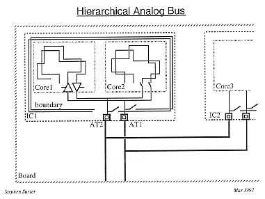
Refer to Viewgraph VG20: Hierarchical Analog Bus. For multiple cores
inside an IC1, all cores will share the same TAP which is universal. What
is different from core to core is the presence of the 2 switches as shown
in the diagram. Ken pointed out that some ICs have 1149.1, P1149.4 or neither,
and the question is how to handle that. At the board level, we all know
what to do. But in a MCM, it is little blurry. Inside an IC, we need a
"cookie cutter" on a smaller scale. Each will have their own
TAP. Adam Cron suggested to deal with the multiple cores as a separate
issue and instead focus on just how to get scan data into the chip. The
point is to avoid excessively high leakage by each core with each having
its own AT lines. If you need a large number of analog signals, P1149.4
is, at this stage, not ready. Steve said there are almost no changes needed
in the P1149.4 document. The two switches may be closed to reduce leakages
in a core. If there were 1000 pins in the boundary, then more than one
TBIC is needed. Adam asked what controls the two switches, Steve replied,
"with a bit". Leakages will occur only in the interior of the
core. The two switches are TBICs that we have been talking about. TBIC
switches have small capacitance but can quickly add up with an increasing
number of TBICs. Steve said a formal proposal is on the next viewgraph.
Refer to Viewgraph VG21: Solved Analog Bus Problems. This is not yet
a formal motion. A TBIC can be hardware or software controlled. One can
only monitor one voltage at a time on AT2. CJ said it is good that hierarchy
issues are brought up. When signals are fed into an IC, what happens? Any
scan chain? The answer is no. There are no ABMs inside the internal cores.
But what is enclosed by the boundary of the IC1 (in the previous viewgraph)
is what we consider an ABM. Adam Ley said this is the way to stimulate
an analog pin and capture a response. The TBICs, when closed, will be the
only ones closed. As far as document changes, application notes should
be written for these cores. If the boundary scan requires multiple ABs
, what is one to do? For a flat hierarchy, it will work. We need to specify
in the boundary only one AB1 and one AB2, at least for now. However, it
is permissible to have multiple AB1s and AB2s.
At present, there are three types of switches in the Standard. Ken felt
one cannot design the ABM when confronted with the task of developing a
TBIC. Here we don't have the drive requirement or high quality references.
The question now is "what type of switch can a TBIC have"? One
requirement is that the switches employed has to be relatively low impedance
to support high speed testing. Keith also supports this recommendation.
No motion is necessary at the moment. Brian added that for designing TBICs,
use the basic structure of 4 bits controlling AT1 and AT2. 1149.1 will
allow a control cell to fan out. The basic structure is sound. We just
have to write rules for it.
Brian apologized for the fact that the Draft came out shortly before
the meeting and there might have been insufficient time for review. This
Draft has been reorganized since the previous versions. Ken suggested doing
some changes via e-mail. Only major changes have to be done here but the
minor ones may be implemented over the e-mail. In the Draft, the absence
of Figure 3 is an oversight.
The definitions have not changed much. Cross references will be redone
and other editorial tasks will be performed. Brian asked everyone to review
the Draft and send in comments. Without feedback, we will keep moving on
and discussing other things. Steve said a no response is equivalent to
a "yes" vote when balloting time comes. Brian said other people
should get involved too. Up to Chapter 4, no contentious or major changes
in the last few Drafts, including Section 4.4. Ken mentioned about Chapter
5 with some objections from people like Colin to including 1149.1 instructions
that are already discussed in 1149.1. Ken suggested Recommendation (e)
should have "and this standard" inserted at the end of the sentence.
Ken said concerning Page 18, the first sentence of the second paragraph,
does 1149.1 have the same statement? Also, 5.4 and 5.5 should have been
interchanged. The last sentence of 5.6 is now superseded by the event that
took place yesterday. EXTEST Is no longer mandated to be all 0s (per 1149.1
meeting). In addition, differential issue in 5.6 will be discussed over
the e-mail.
Refer to Viewgraph VG22: Differential Output. Steve said it is an "overkill"
having 4 bits but an 8-bit ABM will result in some unused states. The functional
driver shown in the viewgraph can be employed to drive logic 1 and 0.
Is core disconnect an issue? We probably don't want to force both outputs
to same value. We don't always want to drive the outputs to opposite values
either. So, the question is now what? The EXTEST Output States table shown
represents some valid output states. Another concern is that some drivers
can't drive current out of both outputs; only one or the other. Now, the
proposal is that the only state not mandated is same-value outputs (permissible
but not mandated). This is compatible with 1149.1 because 1149.1 drives
from the input of the driver and not from the output side of the driver.
Keith asked why not just have BSDL determine which states are legal or
illegal in the table. 1149.1 addresses differential signals digitally but
not in the analog sense. John Andrews said there is a statement about safety
in 1149.1. Adam Cron said it is probably all right to 1149.1 to establish
some types of rules on differential signals. Ken said we don't have to
worry about 1149.1 objecting to our rules. He said there are legitimate
reasons for not allowing the both outputs to be driven to logic one. Steve
said the point here is there is no way to drive both outputs to both high
and both low. John said there is a class of differential drivers such as
flip-flops that have "q" and "q\" that can have both
high and low. Ken asked that the table be clarified. What we know is that
tri-state is mandated in P1149.4. Grady Giles said 1149.1 did not mandate
tri-state.
Brian proposed we hold further discussion on the differential topic.
John said perhaps descriptions may be included in the Draft. He said P1149.4
does a good job with differential but 1149.1 did not really deal with differential
pins. Steve said this is the only nagging topic left in differential. In
short, the question remains: Should we option the possible state of both
outputs having logic 1 to allow for room for possible future applications?
Would source followers placed at both outputs solve the drive strength
issue? Ken asked how one can discriminate between a stuck-open fault and
a perfectly legal high state? Issues like these led to the topic being
delegated to e-mail discussion.
John Andrews said in 1149.1 it is required to have a boundary scan cell
at the output of a receiver, but not in P1149.4. Steve said it's optional
in P1149.4 as it stands now. Keith and others would like to see it mandated
to make it compatible with 1149.1. Brian said he will write up the section
on differential. It will be under the ABM section.
More changes to the March 1997 version of the Draft. On Page 25 replace
"+" with "-" in Note (e), the first parenthesis. Delete
"virtual" from Note (e) (2). Make (e) a Recommendation (a good
design practice). Note (e) (2): A simple inverter is not what is desired
here, instead use a simple NAND gate (which always has a defined output).
Note (2) is probably too short for this explanation. The point here is
you can implement a device simpler than comparator.
Page 26: Description, second paragraph, change "will" to "may"
because of the possibility of different technologies of TTL, ECL, etc.,
being used. The rationale for the paragraph is so we may use EXTEST of
1149.1 to do 1149.1 interconnect tests. We don't want to sound like all
AT1s are/should be connected together.
Page 31, Second Paragraph: Adam Ley asked if everyone agrees on the
term "DBM". Adam Ley and Lee Whetsel said it doesn't hurt to
reiterate the definition of DBM (implying it's already been defined in
1149.1; delete "which defined in 1149.1" from the first sentence).
Page 31, figure at bottom of the page: Discussion on how to "marry"
1149.1 and P1149.4. Basically, it is necessary to reword in 1149.1 to not
disallow this alternative form of boundary scan register. Ken said if we
support 1149.1's INTEST, then the structure on the right is permissible.
Section 7.2 was explicitly accepted by Colin.
Page 33, Note c) (2): Delete the entire contents inside the parentheses.
Furthermore, 2) (d): Add "For the instructions defined herein"
and delete "the contents of the ABM register". Keith mentioned
the survival of chips in short circuit situations, i.e., we should include
issues involved in making a switch (in the Definitions Section?). Brian
said this is discussed in chapter 9, Practical Considerations.
Page 34, 2) (h): This issue was delegated to e-mail discussion as there
were still unresolved issues. Permission (i): Replace "shall"
with "may" and add the word "both" before "AT2"
since a reference may be supplied by a DAC.
Page 35: Steve said we don't want to disallow the use of two voltage
references. The issue is tabled for e-mail since this same topic was discussed
in the morning without a satisfactory resolution.
Page 37, the Table: The key thing that can be added here is to be able
to drive AB2 and AB1 to Vh and Vl.
Page 38: Boundary scan register is a parallel input-output register.
The shift path doesn't go through the cells. Interested readers should
consult the 1149.1 document to verify this.
Page 39, the figure on bottom of page: There are various ways to implement
this (global instructions, etc.). CJ suggested to get rid of "control"
in the control register. Steve pointed out that only mode 1 and mode 2
go to other chips but not data, control , BUS1 and BUS2. More changes will
be made to the diagram.
Pages 40-41: The pictures and references are a bit inconsistent. Brian
will fix them.
Brian will modify Chapters 6,7, and 9 extensively and put D12 out soon.
He solicited comments and review.
There are about 50 people in the balloting group. Adam showed viewgraphs
consisting of a long list of the registered balloting members. He received
an e-mail message from Pat McHugh (Viewgraph VG23). On April 15, the balloting
group will be closed (45 days after mailing). On May 15, ballots will be
mailed from the IEEE (1 month lag usually). July 15 is the ballot return
deadline (60 days from mailing or 75% returned). If no comments, the Draft
will be submitted by the August 5th deadline for the September Standard
meeting. Approval by the ITC time frame.
If comments are received, one month will be allowed for resolving comments
(August 15). Another month is permitted for mailing resolved ballots (September
15). One month is allotted for further comments (October 15). Completion
in time by the November 5th deadline for the December Standard meeting.
There are some participants in P1149.4 that are not eligible because they
are not IEEE members. Adam will send out e-mail balloting forms and will
also e-mail a list of all eligible voters.
CJ reports on the status of 1149.1. The 1149.1 Working Group is trying
to get the Draft reviewed and balloted. Differential issues were discussed
and the Whet-cells were added. 1149.1 acknowledged Dot-4 by adding two
extra bits.
Possible next meeting locations: IMST '97, Tuesday, June 3, 7 a.m.,
to noon Friday, June 6, Seattle, WA, at Mani's house. Last year the Workshop
was held in Quebec City with about 100 people attending. Two years ago,
approximately 150 people participated. Adam Ley asked how this is aligned
with the balloting. Brian suggested to do it at HP in Colorado with
Ken Parker and John McDermid available. Steve volunteered San Jose to be
site of the meeting. Adam Cron said Illinois is another possibility. Keith
said the East Coast is good. This issue will be decided through the e-mail.
Adam said we will not go to ballot by April 15th, as Pat McHugh suggested.
Instead, Adam is shooting for an ITC ballot. Steve likes ITC also because
we can advertise to test engineers and this year's theme is mixed-signal
testing. Brian said wherever it be, should be convenient to the people
who do contribute. Steve said the next WG meeting is past the point of
making significant changes. We can go to ballot in June and deal with the
resulting comments at the next meeting.
Seconded. Unanimous approval. Meeting officially adjourned.