for
October 20, 1996
| Time | Topic | Responsibility |
|---|---|---|
| 8:00am | Continental Breakfast | |
| 8:00am | Arrival and Introductions | Adam Cron |
| 8:15am | Approval of May, 1996 Minutes | Adam Cron |
| 8:30am | Number of Bits in Register | Lee Whetsel |
| 9:15am | BSDL Proposal | Ken Parker |
| 10:00am | Break | |
| 10:30am | New Test Chip Design Effort | Akira Matsuzawa Katsuhiro Hirayama |
| 11:30am | IC Test Progress | Keith Lofstrom |
| 12:00pm | Lunch - Thank you Panasonic | |
| 1:00pm | Draft Review | Brian Wilkins |
| 3:30pm | Break | |
| 4:00pm | Software for Test Chip | C.J. Clark |
| 4:15pm | Officer Affirmation Vote | Mani Soma |
| 4:30pm | Chapter 8.4: Switches, Vref, and ESD | Steve Sunter |
| 5:00pm | Ballot Status | Adam Cron |
| 5:15pm | Next Meeting at ITC | Adam Cron |
| 5:29pm | Miscellaneous | Adam Cron |
| 5:30pm | Adjourn | Adam Cron |
| Working Group Members | 36 |
|---|---|
| Total Subscribers | 341 |
| Total Subscribers on "esd" reflector | 253 |
| Countries Participating | 32 |
| Companies/Universities Participating | ~214 |
| Funds Available | $876.79 |
| Name | Company Sponsor |
|---|---|
| John Andrews | National Semiconductor |
| Terry Borroz | Teradyne, Inc. |
| John Braden | Stratus |
| CJ Clark | Intellitech |
| Bill Coombe | Medtronic |
| Adam Cron | Motorola |
| Dan Dandapani | University of Colorado |
| Craig Danes | Guidant/CPI |
| Ted Eaton | Intellitech |
| John Ford | Silicon Systems |
| Ren Franse | Panasonic Semiconductor |
| Yasuo Furukawa | Advantest |
| Allen Heiden | Motorola |
| Katsuhiro Hirayama | Panasonic Semiconductor |
| Terry Junge | Seagate International |
| Jake Karrfalt | Alternative System Concepts |
| Adam Ley | Texas Instruments |
| Keith Lofstrom | KLIC |
| Akira Matsuzawa | Matsushita |
| Colin Maunder | BT Laboratories |
| John McDermid | Hewlett-Packard |
| Math Muris | Philips |
| Naveena Nagi | LogicVision |
| Elbert Nhan | Johns Hopkins University |
| Kozo Nuriya | Matsushita |
| Adam Osseiran | Ecole d'Ingenieurs de Geneve |
| Ken Parker | Hewlett-Packard |
| Adam Sheppard | ASSET InterTech |
| Mani Soma | University of Washington |
| Steve Sunter | LogicVision |
| Tony Suto | GenRad |
| Jon Turino | Integrated Measurement Systems |
| Lee Whetsel | Texas Instruments |
| Harry Whittemore | nCHIP |
| Brian Wilkins | Southampton University |
| Tom Williams | IBM |
| Name | Company |
|---|---|
| Steve Dollens | International Microelectronic Products |
| Michel Parot | Thomson-CSF |
Adam Cron and the WG thanked Panasonic for sponsoring today's meeting
(approximately $52 per person for food and refreshments). Adam announced
there would be a P1149.4 technology demonstration for interested people
on Tuesday, 10/22/96, in the same room (Idaho) from 3 to 6 p.m. Introductions.
Review meeting agenda. Keith Lofstrom was set to present two papers on
Tuesday afternoon and Wednesday morning. Ballot: Invitation was not closed
yet, and therefore more can still be added to the ballot list. Adam reiterated
the voting policy: only WG members may vote.
Approval
of October, 1995 Minutes
Adam received a motion to approve the 05/96 minutes. Seconded. Unaminous
approval.
Before turning the stage over to Lee Whetsel, Adam said he would like
to have a consensus in the WG on the number of bits in the Standard.
The motivation for this proposal is to standardize the definition of
a test cell in both 1149.1 and P1149.4. The analog test cell is similar
to the digital test cell in 1149.1. The task is to come up with a definition
without significantly changing the analog boundary module (ABM) with its
digital functions already well defined.
Viewgraph VG1: Example P1149.4 Test Architecture.
Steve Sunter said there is no switch between the output of 3SOA and the
output pad, looking at the internal structure of the analog test cell (ATC)
on the viewgraph. Lee said P1149.4 interconnect testing includes the capability
of testing wires, inductors and resistors, and checking capacitors for
shorts. The P1149.4 interconnect test also covers high and low termination
drive tests.
The following viewgraphs show the various proposed analog test cells
for 1149.1.
Viewgraph VG2: 1149.1 2-State Analog Test
Cell. This 1149.1 analog test cell will not support the full P1149.4 metrology
since no tri-state is available, but it is compliant with all other 1149.1
instructions.
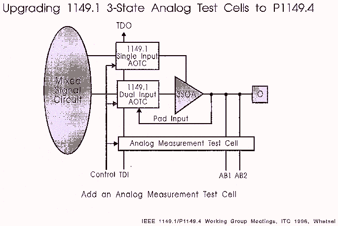
Viewgraph VG3: 1149.1 3-State Analog Test
Cell. This modified 1149.1 analog test cell supports full P1149.4 metrology.
With the addition of a single-input analog output test cell (AOTC). Tri-state
for 3SOA is enabled through the single-input AOTC.
Viewgraph VG4: 1149.1 Bidirectional Analog
Test Cell. This ATC is similar to the 1149.1 bi-directional digital test
cells. Capture Select (CS) is used during Sample/Preload. This ATC is compliant
with all 1149.1 instructions.
Viewgraph VG5: 1149.1 Input Analog Test Cell.
This viewgraph shows a proposed 1149.1 input ATC that is similar to the
existing 1149.1 Capture-Only Digital Test Cell.
Viewgraph VG6: 1149.1 Buffered Analog Test
Cell for Signals Without Functional Output Amplifiers. Test output buffer
(TOB) provides strong test drive and reduced test loading. Ken Parker asked
how strong the buffer has to be. The identity of the pin might be different
in the normal mode and the test mode, and P1149.4 assumes that. Lee would
like to see it shown as an example in the Standard. Keith joined the discussion,
saying we are arguing over something that is imaginary. Treat it as a black
box (we should not care whether the implementation is a transmission gate
or a buffer). Keith pointed out an amplifier/buffer has stability problems
if it is not carefully used. Buffers are neither required nor precluded
in the Standard. John McDermid asked if there is a V- for return. Lee said
yes. He added that this is not for measurement, but for setting up test.
John was concerned about the buffer having offset and stability problems.
Sunter said we can only specify what can be measured off-chip, not what
is inside. We are dealing with implementation details here!
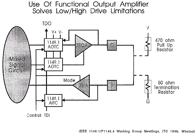
Viewgraph VG7: Use of Functional Output Amplifier
Solves Low/High Drive limitations. This slide shows 1149.1 analog interconnect
test examples. The output amplifier may be employed to handle 50-Ohm termination
resistor and 470-Ohm pull-up resistor loadings. Again, whether a transmission
gate or a buffer should be used is an implementation issue.
The following viewgraphs deal with the various methods to upgrade 1149.1
chips and test cells to P1149.4.
Viewgraph VG8: Upgrading a Chip from 1149.1
to P1149.4. To transform a chip from 1149.1 to P1149.4, all one has to
do is add an ABD, AT1 and AT2 pins (to make a 6-pin TAP), analog measurement
test cells (AMTCs), and internal AB1 and AB2 bussing.
Viewgraph VG9: Upgrading 1149.1 2-State Analog
Test Cells to P1149.4. To add tri-state feature, replace the amplifier
with a 3-state amplifier, add an analog measurement test cell and a high-Z
control. Ken asked what the difference is between a 4-state cell proposal
back in 1993 and this one. He would like to see separation of analog and
digital test cells. A 3-cell structure is probably more difficult to implement
than one with 4 cells. Ken said the elegance of separation is that it appeals
to 1149.1 WG, and is easier to convince those folks. Adam asked what then
if we have a stability problem with a 3SOA? Lee said this is a design/engineering
issue. Lee wanted to keep the cell as simple as possible and assume good
engineering practices.
Viewgraph VG10: Upgrading 1149.1 3-State
Analog Test Cells to P1149.4. One only has to add an AMTC in this case.
Viewgraph VG11: Upgrading 1149.1 Bi-Direct
Analog Test Cells to P1149.4. This scenario only requires the addition
of an AMTC.
Viewgraph VG12: Upgrade 1149.1 Buffered Analog
Test Cells to P1149.4. Simply add an AMTC. Ken commented that there is
a design constraint on the buffer.
The following viewgraphs present upgraded 1149.1 measurement examples:
Viewgraph VG13: Once upgraded from 1149.1
to P1149.4, when measuring a resistor, disable 3SOA using an AOTC control;
output V- from AITC's 3SOA to sink Idc; force a known Idc through the unknown
R to V-; then close the AB2 switch of the output to measure V2 and close
the AB2 switch of the input to measure V1. John said some devices don't
come with ground. Terry Junge said a power pin can be used instead of a
ground pin. If test cells can truly be shared between 1149.1 and P1149.4,
things will be simplified significantly. Steve Sunter asked if there is
anything in P1149.4 that would preclude the implementation of this scheme.
Lee said he wasn't certain. Steve said as the draft stands, nothing prevents
us from using this scheme. Adam Cron wants the number of bits mandated
so that Brian Wilkins can write it into the draft. Brian asked if 4 bits
are now mandated.
Viewgraph VG14: Required Step to Standardizing
Analog Test Cells Between 1149.1 and P1149.4. A P1149.4 ATC must be partitioned
into 2 cells (1149.1/P1149.4 ATC and P1149.4 AMTC). A 1149.1/P1149.4 ATC
satisfies 1149.1's input, output and Input/output interconnect test requirement.
A 1149.1/4 ATC in combination with P1149.4's AMTC support full P1149.4
measurements.
Viewgraph VG15: Obstacle Confronting Development
of Standardized Analog Test Cells between 1149.1 and P1149.4. To partition
1149.1 and P1149.4, it is necessary to eliminate decode and add another
cell. Adam said he wants a motion on the number of bits. Ken suggested
to wait until end of the day to vote on it so that other parties may present
their materials and viewpoints that may have a bearing on the outcome of
the vote. Steve asked what the advantage of this scheme as a user (chip
designer) is. Lee said 3-bit will not allow partitioning but 4-bit will.
One advantage is to get 1149.1 and P1149.4 on the same page. It would simplify
matters considerably. Lee reemphasized that standardizing is the prime
objective of his proposal.
BSDL was rewritten in 1993 (with lots of pain and grief). If standardization
is dealt with and handled properly, it would make life infinitely easier
for software. The issue here is more on what it takes to support the Standard
(to create a viable standard), and not so much on the standpoint of saving
silicon and so forth. In a standard such as P1149.4, software is equally
important as hardware.
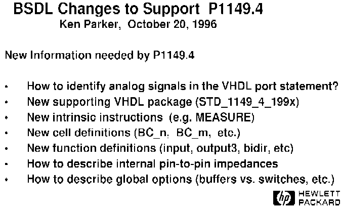
Viewgraph VG16: BSDL Changes to Support P1149.4.
In the current draft, there is presently nothing on 3-bit vs. 4-bit. From
the software standpoint, the number of bits is important to know and should
be mandated. If software development costs can be amortized over a large
number of people, that would be ideal. People rely on the standard. The
software needs to know what to do for a standard. It needs to know how
to get data from measurements and process it. We must provide the software
designer with rock-solid definitions and language to create useful and
meaningful test software. BSDL is a subset of VHDL. BSDL, until a few years
ago, completely ignored analog pins. It treated analog pins, no-connects,
power, and ground pins as "linkage" pins (essentially "garbage"
pins that were ignored). One approach is to include analog pins and then
figure out how to handle them later. The P1149.4 Standard has new terms
that require new definitions. There is probably even a need to add new
functions; anything but optioning the new features in P1149.4. The reason
is that the optional features will grow and eventually become excessive
as will the software. If an ABM is an amorphous object in terms of not
having the number of bits specified, then there will be problems. It doesn't
matter if it is 3- or 4-bit, we need to nail it down. Between Keith and
Panasonic, we will hear about an experience concerning real silicon test
chips. A question was raised about whether BSDL was written only because
the number of bits was mandated in 1149.1. The answer is yes. Whenever
you add an option, the complexity of the software correspondingly increases.
If there was no limit to the number of bits, then a viable and practical
standard cannot be written. In Chapter 10 of 1149.1, it looks complicated
for software but is actually implementable. Ken proposed that we identify
each flip-flop with a purpose and a name. If pins cannot be identified,
then it is impossible to produce software. Ken wanted to make a short list
that will solve all the important problems. There is also global options
vs. per-pin. A logical question is: if VHDL has a way to handle this, should
we use it for BSDL? Ken said he had bad experiences with it. A question
was raised about the 1076 and whether we need to take a look at it. Adam
asked if we should go to ballot without BSDL. Ken said this would be better
answered later.
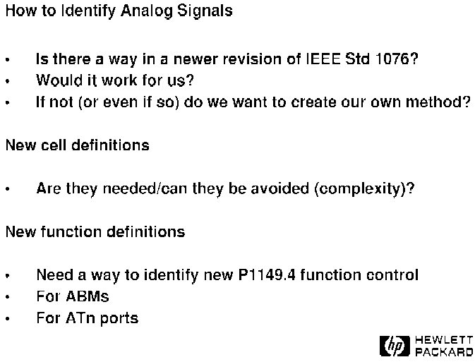
Viewgraph VG17: For P1149.4, there will be
new function definitions. A way to identify new function control. Ken said
if we followed the elegant way to extend 1149.1 into P1149.4 , then the
software should follow very quickly.
Viewgraph VG18: How to describe pin-to-pin
impedances. In the Standard, guidelines will be provided, but at what point
should we say the user is allowed to do this but not that. As an example,
when measuring resistors from pin to pin, what if a FET is in between?
What about global options? Are they all-encompassing? Are there any exceptions?
It is evident that this is a complex issue. With that, the floor is open
for discussion.
Software has to be written in a very concise way and the standard has
to reflect that. Reviewing the draft is important for people such as Panasonic
and Keith. A lot of people out there will have only a draft to look at.
Therefore, it has to be unambiguous. Keith pointed out that we can't restrict
too much on the mission circuits. There are people out there that still
leave pins out of 1149.1 chips and we have to tolerate it. The same thing
is predicted to happen in P1149.4. The Standard says to do it a certain
way, but the market determines the winners and losers.
A motion was on the table: We will go to ballot prior to defining BSDL
for P1149.4 Standard - Yes or No? Seconded. Discussion followed. It took
3 years to write BSDL and no one now cares anymore. Modified motion by
adding the word "formally" before "defining ....."
Brian said the real reason for the delay of the draft is nobody devotes
full time to it.
MOTION: We will go to ballot prior to formally defining BSDL
for P1149.4 Standard. Seconded. Yea: 16. No: 0. Abstained: 0. Unaminous
approval.
MOTION: We will define a BSDL for P1149.4 Standard. Seconded.
Yea: 17. No: 0. Unaminous approval.
Before going to ballot, we need to at least clearly define the number
of bits. We can write BSDL today, if we wanted to, that will do interconnect
tests. Balloting will sound an alarm to the industry that a standard is
being established and will probably lead to more critical reading of the
draft that will result in feedback and data for the WG. Adam asked if we
can write BSDL for draft 10 as it stands today. The answer is no.
Viewgraph VG19: The complete specifications
for the MEI test chip (MNABST-1) were distributed in handouts. The objective
is to evaluate the analog test bus structure with various switches. This
chip is fully compatible with 1149.1. Only basic functions (Bypass, Sample/Preload,
EXTEST) are implemented.
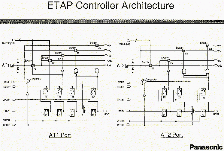
Viewgraph VG20: Shown is the ETAP controller
architecture for the test chip MNABST-1.
Viewgraph VG21: The analog boundary module
is shown. The diodes at the pin and core are ESD protection diodes.
Viewgraph VG22: A photograph of the evaluation
board.
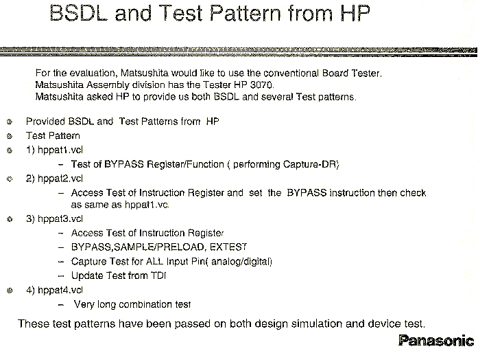
Viewgraph VG23: Matsushita tested the chip
using BSDL and test patterns (which were distributed on the reflector by
Ken) provided by HP on an HP3070 tester. The test patterns were successfully
used to test the chip.
Viewgraph VG24: Why was MNABST-1 implemented
using 0.35 micron process? Because it is a conventional process and Matsushita
expected it to be the most widely used process. In addition, 0.35 micron
CMOS serves as the base for future deep quarter-micron process and therefore
there are merits to experiment with the 0.35 micron. Experiences gained
from working with the 0.35-micron can be applied to the quarter-micron
process.
Viewgraph VG25: Shown is the complete chip
layout with the various metal layers. A question was raised about the number
of metal layers implemented. The answer is 3 for now, 5 in the future.
Viewgraph VG26: Size estimation. By optimizing
the chip layout for the differential comparator (VG25)
resulted in a space saving of 8% using .35-micron CMOS process for one
ABM. When optimizing, 100-Ohm resistance value was selected out of 4 possible
values.
There are layout restrictions for an ABM. In a deep submicron process,
the metal conductor resistance increases because of the decrease in width.
This can possibly affect measurement results. The total path resistance
is 43 Ohms. In short, the guideline for layout must be observed, i.e.,
the pad-ABM interconnection has to be laid out as short as possible. Steve
said there is no need for these guidelines if using 2 wires. For P1149.4,
the cost of wiring will be higher than for 1149.1.
Viewgraph VG27: Distribution of evaluation
board, BSDL, and specifications. The test chips will be available only
to P1149.4 WG members free of charge. Interested individuals should fill
out a registration sheet provided by MEI. Forty sets are available at present.
Test chip recipients are requested to report any results to P1149.4 WG.
For requests from within the U.S., contact Hewlett Packard. Test chip requests
will be filled for requestors outside the U.S. by MEI. One condition attached
to the receipt of these test chips is that they are solely for P1149.4
evaluation purposes.
Viewgraph VG28: The on-resistance of a 120
Ohm analog switch is 70 Ohm. For 2 KOhm resistors, the on-resistance is
1.6 KOhm. For N- and P-channel switches, the on-resistance increases as
a function of the gate voltage. The resistances increase to 120 Ohms and
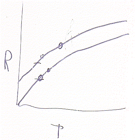
11 KOhms, respectively, at a voltage of 2 V. The gate on-conductance is
maximum at 0 V gate voltage and is minimum at about 2 V. Fluctuation of
switch impedances at low voltage levels is an important issue. A thorough
understanding of the behavior of the on-resistance at low voltages is required
to avoid obtaining erroneous or extraneous measurement results.
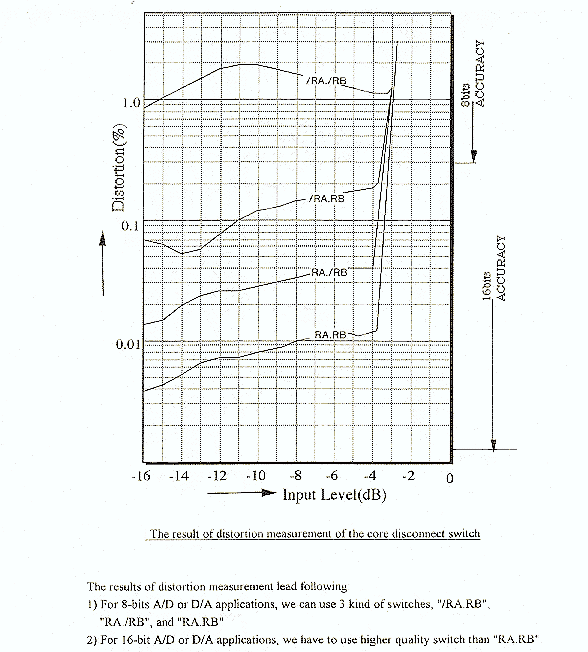
Viewgraph VG29: Distortion measurement of
the core-disconnect switch. The distortion is approximately 1% for 8-bit
accuracy and 0.01% for 16-bit accuracy. The point here is to select switches
with appropriate distortion levels. The designer should choose several
types of switches. The offchip load impedance is 1MOhms.
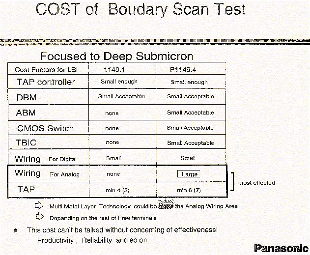
Viewgraph VG30: Cost of Boundary Scan Test.
This is a table comparing the cost factors between 1149.1 and P1149.4.
For 1149.1, the cost is minimal and the TAP controller and DBMs can be
made small in submicron technology. However, P1149.4 requires large wiring
area which can be reduced using multi-metal layers. In short, P1149.4 will
require more silicon and may cost more than 1149.1.
Ken said that the chips have been available for 2 months now. There
was a demonstration of the MEI chip on HP tester at the HP booth at the
ITC. The demo performed indicated that 1149.1 interconnect tests work with
1149.1 BSDL. The HP P1149.4 exhibit at the show included demonstration
of measurement techniques for a 1.5-mH inductor (to an error of less than
1%) and a 10% capacitor. Also, measurement of a 3-resistor delta was performed.
Parasitic impedances caused the measurements to be a little high. There
were also AC measurements. The demo used 1.6-KOhm switches. With this arrangement,
very low resistance values can be obtained. The objective here, again,
is to test out the P1149.4 metrology. Ken invited everyone to stop by the
HP booth. More experiments were to follow.
Adam thanked MEI/Panasonic for the test work.
Keith will have presentations this week. Keith used 1.2-micron process
(but have 1.5-micron cells). The ETAP is "crummy". The emphasis
was on time and not so much on creating a perfect chip.
Drifts during test: The conventional wisdom that one can obtain more
accuracy in test if averaging is used is not necessarily true. On a blank
viewgraph (VG31), Keith illustrated the variation
of switch resistance with time. There are stored charges in silicon that
move around which can affect switch resistances. Averaging can actually
make it worse since there is more time for resistance to drift. Averaging
can mask random noises but cannot shield drifting resistances. Thermal
effects along with mobile charges and other factors are responsible for
resistance drift in MOS. Keith reported a 0.3% measurement error with not-so-great
equipment. One can run production types of tests with PCMCIA and a laptop,
which is great for field engineers. Keith mentioned he came across P1451.2
standard which basically is a smart transducer interface for sensors &
actuators. Stan Woods of HP is the contact if more information is desired.
Steve Dollens' demo board hasn't been scanned through yet.
The software for interfacing with the board used to be available on the SPAsystem.
If anyone is interested in experimenting with Keith's software, then get his from him.
Draft 10 had been e-mailed to the reflector. We should base the draft
on the most current revision of 1149.1 and thus we should remove the "P1149.4
must follow 1149.1" phrases. A better way to say it is "we are
consistent with 1149.1". Lots of changes have been proposed to 1149.1
but they have not been written in yet. Whenever 1149.1 is updated, P1149.4
will also be. Ken mentioned he sent out an e-mail last week with philosophical
statements about P1149.4 and 1149.1 compatibility (i.e., if protocols are
compatible, then the same algorithms may be adopted). Section 1.2 addresses
that. But Brian wanted to address the issue that if a chip is 1149.1 compatible,
does it mean all rules of 1149.1 apply to it? The bottom line is: Brian
will synchronize the P1149.4 draft with the latest version of 1149.1 instead
of "known changes" that WILL be made to 1149.1. No motion on
this discussion is necessary.
A motion was initiated by Lee Whetsel on having an ABM consisting of
2 distinct cells -- digital and analog.
Ken said 1149.1 has a number of ways to deal w/ bidirectionality. Brian
said we are removing requirement to use 3 bits (cells) with the option
of having an unlimited number of bits. The next motion will focus on defining
the function of each bit. Colin said 1149.1 only specifies functions, not
implementation details. Debates on whether it is important to define bit
functions ensued. Ken said 3 bits vs. 4 bits means measurable overhead
and likes the separability of 1149.1 & P1149.4 cells. More debates
followed. Steve said AMODE is an option whether we have 3 bits or 4 bits.
ken said 3 bits, yes, AMODE is required because 3 bits plus AMODE will
be necessary for all 11 states. Some spare states are available for production
IC parameter testing. Control cells cannot be shared in P1149.4. Instead,
P1149.4 needs dedicated controls. Brian urged to close this discussion
so that the motion can be voted on.
MOTION: The P1149.4 analog boundary module will comprise 2 separate
cells:
Seconded. Yea: 15. Nay: 0. Abstained: 0. Unaminous approval.
Terminology: Ken said in P1149.4, we call a group of cells analog boundary
module. Colin said basically we are using 1149.1 DBM to describe something
not existent in 1149.1. The word "cell" raises a lot of confusion.
An ABM has both a digital and an analog section. Adam asked if we can delete
Section 8.2 in the draft. This is an editorial issue. Adam suggested to
adhere with the term "DBM" and proceed onward. Steve disagreed
saying that it would create a "mess" if we equated a DBM to a
digital boundary cell.
More on terminology: Core circuit vs. system circuit. The only concern
is that the circuit is not just digital but analog also. Colin would like
to see consistent terminology in both 1149.1 and P1149.4 eventually. Thus,
use "core circuit", "core disconnect" as in 1149.1.
Another issue: Differential signals (John Andrews). These signals exist
in analog, digital and mixed-signal circuits. Brian drew on a viewgraph
(VG32) a diagram of 2 chips interconnected with
ATC's. Scenario: If we have to test the recommended ABM's (denoted by "R"),
should we use the PROBE instruction. Colin suggested 2 types of EXTEST
instructions, one for digital and the other for analog. Adam asked if anyone
wanted to make a suggestion on the optionality of the recommended register
and instruction. In a sense, it could be treated as an EXTEST. In 1149.1,
each digital differential pin is a digital pin. However, in P1149.4, the
mandated cells take precedence over the recommended cells. The fact remains
that we need to consider and take into account testing in noisy environments.
Steve said we have resolved this issues before. The Ms on the viewgraph
represent ABMs.
It was suggested to form a subgroup that focuses on the issue of whether
to have DBCs for the Rs in the diagram. Adam recommended that Steve Sunter
and Brian Wilkins get together and decide what they should be (ABM or ABC,
etc.). The bottom line is to standardize the terminology.
Instruction issue: Lots of disagreements here. What do we mean by INTEST?
Do we need to have it? Lee said yes. 1149.1 has INTEST. Is INTEST worth
defining? Lee said yes. If so, what does it mean then in a P1149.4 chip?
Ken asked if the INTEST instruction is loaded, should core disconnect be
open or closed? When open, the ABMs on the pad side are disconnected from
the mission circuitry. Maybe we need to caution that INTEST is really defined
only in 1149.1 and one should be careful every time INTEST is loaded to
make sure the chip does not get damaged. INTEST has to be defined unambiguously
because of the digital and analog interface. Adam asked if anyone wanted
to work on the INTEST issue. Subsequently, a subgroup consisting of Lee
Whetsel, Keith Lofstrom, Steve Sunter will hash out the topic of INTEST.
Core disconnect (CD) on input pin: Do we need to mandate CD on input
pins. Steve said we have not mandated a physical switch there but do require
anything that happens outside chip will not affect chip. From the outside
world, one cannot tell if there is a switch in the chip. Keith suggested
to always show an explicit switch to avoid confusion. Lee said an output
pad does require a conceptual switch but an input pad does not. Lee is
not comfortable with Figure 15 in the draft and will work with Brian on
it.
Steve does not have any new presentation on current/voltage buffers.
If there is a current on AT1, a voltage on AT2, how do we handle that?
This issue was deferred to e-mail discussion. Steve said it is more efficient
to debate over the e-mail and then vote on proposals in WG meetings. Brian
said it would help if some other people would also contribute. CJ preferred
to discuss the proposals complete with pictures and diagrams in WG meetings.
Adam said he can put pictures on the web if necessary.
Ken referred to Figure 10 on pages 9 to 11 in the MEI test chip specifications
document. He suggested to consider this concept of an AT port. Here is
a physical implementation that works and should be a valuable addition
to the Standard. There are currently no measurement instructions. EXTEST
can do the basic tests, and if complex testing is required, then we add
options (e.g., for bipolar). The consequence is that different flavors
of EXTEST (e.g., measure) can be invented for various purposes.
Ken started the discussion of an AT port having a boundary scan cell.
Steve said at one point we had that but it somehow dropped out. EXTEST
connects TDI and TDO but also AT1. Pages 9-11 of the MEI specifications
document show one implementation that potentially has some good capabilities.
Action Item: Ken will help Brian make the 4-cell scheme more
consistent.
Anyone interested in reading PostScript format should visit this site:
http://www.cs.wisc.edu/~ghost/.
This web site contains downloadable software that interprets PostScript,
GhostScript, GSView, etc.
CJ thanked Lee for pushing for a 4-bit ABM. A 4-bit ABM would really
help today. He has been working on demo software along with Ted. CJ had
problems with tables 2 and 3; working with 1149.1 ASSET Software. In this
situation, one cannot just take a regular 1149.1 tool and do whatever desired.
The software needs to be modified. The bottom line is that there was a
major change in today's meeting -- 4-bit ABM. Lee solved the problems.
CJ was to demo the software at the show. CJ wirewraps his own board for
use in testing out his software.
Regarding the demo board issue: It was interpreted in a different way.
It should be noted that CJ's demo software will not work with Steve Dollens'
board. CJ said the boards should just be given to WG members. His software
will work with 3-bit or 4-bit cells.
It is ballot time. Nominations for Chair, Vice Chair, Editor, and Secretary
are the incumbents. A motion was initiated to approve the elections for
1997:
MOTION: The above officers for P1149.4 Working Group for 1997.
Yea: 13. Nay: 0. Abstained: 2. Motion carried.
Steve had sent Brian's request for ESD requirements over the e-mail.
Viewgraph VG33: Electro-static discharge
protection. In the diagram on VG33, Rcom cannot
be cancelled out or calibrated for measurement. Rcom represents the 43-Ohm
path resistance on the MEI/Panasonic test chip. When forcing a current
through AT1 and AB1 and monitoring the voltage at AB2, assuming a small
current through resistors, then accurate measurements can be obtained.
We should make sure Rcom is less than 1 Ohm for 1% accuracy. If this structure
was connected to another similar structure, then would the accuracy of
the reading be 2%? The answer is yes. Rcom depends on the output driver
impedance. This rule is very design dependent. MEI thinks this scheme is
reasonable. This Rcom is the "undocumented" resistance. If any
more impedance is added, we would need to document it (this was agreed
upon and was one of the results from the switch subgroup meeting). Draft
D10 does not have any implementation details. However, some examples will
be included. Mani asked continuous technology improvement will demand the
requirement to be less than 100 uA. The total resistance from AT1 to the
pin should be limited to 10 KOhms. Rload should be than 1 KOhms. These
are just wire resistances, not physical resistors. Lee pointed out this
is midband model. If a resistor is in series, that has to be documented.
If the path resistance met specifications, it does not have to be documented.
Otherwise, it would have to be. If Rcom can somehow be bypassed, then no
documentation is necessary. Adam Ley summarized the main point of this
discussion: The rule is such that if the path resistance does not meet
the specifications as given, then it must be documented. One ESD resistor
is needed for driver, and another for the entity being driven. Adam Osseiran
asked if we are talking about CMOS here. The answer is no. Ken added that
this is for the general case for ESD which is independent of technology
being employed.
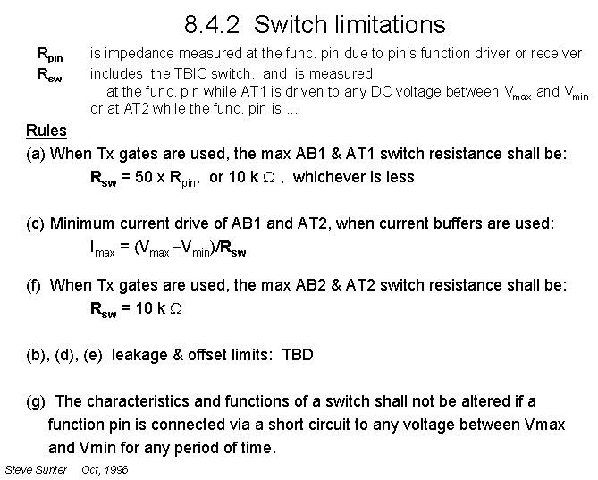
Viewgraph VG34: Switch limitations. Debates
and discussions resulted in the following modified form of switch rules:
Rpin is impedance measured at the func. pin due to pin's function driver
or receiver. Rsw includes the TBIC switch and is measured at the func.
pin while AT1 is driven to any DC voltage between Vmax and Vmin.
Rules:
This applies to on-chip only, but not on-board. This does not include
bondwires (.1 Ohm). We can document our way around the Rcom but still have
to adhere to these rules. Ken would prefer not to have too many restrictions
placed on the switches that may turn out to be unnecessary or even unrealistic.
However, there has to be some kinds of limits. If a 1 Ohm driver is to
drive a 1 Ohm load offchip requiring a 0.1 % accuracy, then the switch
resistance, as a rule of thumb, has to be 50 times smaller. Lee wanted
to simplify this diagram but this represents actual situations (refer to
VG33).
Action Item: Steve will take this offline with the switch subgroup
on the contents of VG34. As for the materials
in VG33, Brian will attempt to word it.
Terry Junge suggested a guardband by reducing the tolerance to less
than 1%. That is, set the overall impedance to be less than 1%. In this
way, there does not have to be an automatic built-in 1% error. Several
WG members concurred with this point.
To view postscript files on screen, visit the WWW URL mentioned earlier.
Adam Cron will e-mail to the reflector more information. Brian will send
the draft out in postscript and in WordPerfect format. Adam will also accommodate
with the request that ASCII files be made available.
The current head count is 32. Invitation is still open. Just send e-mail
to Adam Cron if interested in being a balloting member. Adam showed a list
of the people currently in the balloting group. There were several omissions
that will be addressed. Adam also showed a list of non-eligible voters
that don't have membership. Ken said we will need at least 100. Other people
agreed. Adam said he can send out another invitation to solicit more balloting
members. Mani asked when the WG goes to ballot. Adam said it was originally
scheduled to be last June. CJ pointed out that 1394 had just gotten approved
after 10 years of standard development. Adam said an EISA Draft Standard
he was just handed was dated 1990. Dan Dandapani suggested sending invitation
to subscribers.
February time frame was suggested. Possible sites and dates were proposed.
Bill Coombe will check if Phoenix is possible in February. He will also
investigate the possibility of a Motorola meeting site (Al Heiden). The
meeting format was tentatively agreed to be 2 half-days.
Ken Parker commended Brian on his work. The Editor position is labor-intensive.
The draft needs to be clear and unambiguous. Ken thanked Brian for his
diligence.
CJ missed the BSDL discussion because of being late to the meeting this
morning. He has already started doing some BSDL and has software for a
3-bit structure. Ken, saying it is an important issue, will talk with his
management at HP and ask that he be able to devote more time to BSDL.
Lee asked how the test chip people feel about the progress? Ken said
for the Panasonic chips, large impedances were employed to drive highs
and lows. There is probably a need for more delay in the capture time.
The pin capacitances were not a major problem.
Adam asked if anyone will do attempt the measurement of the parameters
suggested by Steve Sunter in the meeting. So far, there are no volunteers.
Regarding the next meeting dates. There was a general consensus on the
meeting date not to fall on Valentine's day or Presidents' Day, or any
other holiday, for that matter. The actual meeting dates and site will
be determined over e-mail. Lee suggested we need to target system engineers,
not just designers since system designers do influence chip designers.
Seconded. Unanimous approval. Meeting officially adjourned.