for
May 20, 1996
| Time | Topic | Responsibility |
|---|---|---|
| 8:00am | Continental Breakfast - Thank you Hewlett-Packard | |
| 8:00am | Arrival and Introductions | Adam Cron |
| 8:15am | Approval of February, 1996 Minutes | Adam Cron |
| 8:30am | Switch Definition Meeting Results | Steve Sunter |
| 10:00am | Break - Thank you Hewlett-Packard | |
| 10:30am | Draft D06 Review | Brian Wilkins |
| 12:00pm | Lunch - Thank you Hewlett-Packard | |
| 1:00pm | Draft D06 Review (cont.) | Brian Wilkins |
| 1:30pm | New Test Chip Design Effort | Ren Franse Katsuhiro Hirayamu |
| 2:00pm | Register Length | Adam Cron |
| 2:30pm | New Instruction | Steve Sunter |
| 3:00pm | Break - Thank you Hewlett-Packard | |
| 3:15pm | IC Test Progress | Keith Lofstrom |
| 4:00pm | Demo Software Progress | CJ Clark |
| 4:30pm | Variable Vref, 4 vs. 3 Latches | Steve Sunter |
| 5:15pm | Ballot Status | Adam Cron |
| 5:45pm | Next Meeting at ITC | Adam Cron |
| 5:55pm | New Membership | Adam Cron |
| 6:00pm | Adjourn | Adam Cron |
| Working Group Members | 36 |
|---|---|
| Total Subscribers | 328 |
| Total Subscribers on "esd" reflector | 244 |
| Countries Participating | ~31 |
| Companies Participating | ~181 |
| Funds Available | $2258.84 |
| Name | Company Sponsor |
|---|---|
| CJ Clark | Intellitech |
| Bill Coombe | Medtronic |
| Adam Cron | Motorola |
| Dan Dandapani | University of Colorado |
| Ted Eaton | Intellitech |
| Ren Franse | Panasonic Semiconductor |
| Katsuhiro Hirayama | Panasonic Semiconductor |
| Terry Junge | Seagate International |
| Keith Lofstrom | KLIC |
| John McDermid | Hewlett-Packard |
| Elbert Nhan | Johns Hopkins University |
| Kozo Nuriya | Matsushita |
| Ken Parker | Hewlett-Packard |
| Steve Sunter | LogicVision |
| Tony Suto | GenRad |
| Brian Wilkins | Southampton University |
| Name | Company Sponsor |
|---|---|
| Allen Heiden | Motorola |
| Madhuri Jarwala | AT&T Bell Laboratories |
| Michel Parot | Thomson-CSF |
| Mani Soma | University of Washington |
| Lee Whetsel | Texas Instruments |
Adam Cron asked if anyone had downloaded the Draft D06 and if anyone
had any trouble with it. Nobody seemed to have had any problems. Adam mentioned
an article on the rules for generating a standard draft published in last
month's IEEE Standards Bearer. He announced that C.J. Clark, Ted Eaton,
and Akira Matsuzawa will be eligible to vote in the WG after this meeting.
Adam and the WG thanked Ken Parker for Hewlett-Packard's sponsorship of
this meeting. Adam said because of change in responsibilities, Madhuri
Jarwala could not make this meeting (and probably future meetings). Lee
Whetsel could not attend this meeting due to an impending birth in his
family. Adam said he released the February WG minutes a little bit early
without Bob Russell's viewgraphs, but Bob's proposal was voted down anyway
in the last meeting. Steve Sunter asked how many people there are in the
WG and whether we needed more people for the ballot? Adam said no. The
current WG membership stands at 37. Adam pointed out some people received
yellow ballot forms from the IEEE. Steve commended the February minutes.
Adam motioned to approve the 02/96 meeting minutes. Seconded. Unanimous
approval.
Background: One of the action items resulting from the last meeting
at Seagate was that the switch issue needed to be examined in great detail
since a switch is not just a simple on-off switch. We have core disconnect,
impedances, etc. to consider. A subgroup consisting of Ken Parker, John
McDermid, Keith Lofstrom, Mani Soma, and Steve Sunter was formed for this
purpose. The results from the subgroup study are as follows:
Refer to viewgraph VG1.
Item 1: Impedance is defined as the impedance that can be measured between
two pins (trans-impedance only). Rpin-to-pin (from any analog bus pin to
any function pin) was determined to be less than or equal to 50*Rout, or
less than or equal to 10 kOhms if Rout is greater than or equal to 200
Ohms. A switch impedance is limited to 5 kOhms.
Item 2: There is a need for a very stable current. Voltage references
must also be stable over the duration of a measurement. If one were to
measure a 10-Ohm resistor with a 1 mA current, a reference with at least
100 uV accuracy is required. John McDermid drew on a viewgraph:
A current source delivers a small current (1 mA) to a 10-Ohm resistor.
A voltage reading of 10 mV is measured with a voltmeter across the resistor.
In this instance, the voltage across the resistor must be stable to within
1 uV during the measurement time interval. Keith Lofstrom asked: What about
heating effects? Depends on the length of the measurement time. In terms
of bandwidth, we should measure a voltage between 1 and 100 kHz (the voltage
need only be stable within in this frequency range. We need a Vmin, a Vmax,
and a limit on the magnitude of the current (1 mA is a good number). Steve
asked what limits we should specify (i.e., how do we know if a switch is
big enough?). He said the impedance limit will be a rule, and the voltage
limit can be a rule also (in response to Brian Wilkins' question whether
items 1 and 2 on viewgraph VG1 should be made a rule). Steve said both
impedance and voltage limits (items 1 and 2) will be rules except for the
"1 mA load" and the bandwidth. He pointed out that we need to
give designers some numbers to work with and should not leave the parameters
wide open. Adam asked Tony Suto if this was reasonable. Tony replied that
it sounds reasonable without off-chip capacitance. The 0.001% Vdd must
be between the time the first switch and the second switch are closed for
measurement by the voltmeter (See VG7). Brian asked
what Rout means. Rout means the output impedance of the buffer, and the
switch impedance would have to be 25*Rout on viewgraph VG7.
For core disconnect: the only thing we care about it is the off impedance.
Ken said we need to limit the scope of the "switch" rules to
the basic switches, not including core disconnect. The point here is to
minimize the size of the impedance of switches necessary to implement P1149.4.
It was agreed to delete "+/-1mA load" from item 2.
Item 3: The subgroup members agreed that the switches should be able
to tolerate a short circuit indefinitely between VDD and VSS. Steve mentioned
we haven't put a limit on VDD and VG switches. He said if we mandated that
all pins should be able to tolerate short circuit indefinitely that the
market place would accept it. Adam disagreed (Keith said we could assume
the mission drivers have current limits). Steve said the switches we are
talking about here are parametric measurement switches (i.e., switches
associated with parametric measurements). Steve said there is no mention
about the short circuit capability of function measurement switches (function
and parametric measurements involve different switches). Steve drew on
viewgraph VG7 that G and Vmin are just VL and +V
and Vmax are VH for function measurement. The G and +V switches are used
when in AMODE. In the switch subgroup meeting, only parametric measurement
was discussed, but not AMODE.
Item 4: Turn off a switch in the presence of a short circuit (the statement
was modified by adding the words "able to" to the beginning and
"under scan control" to the end; see viewgraph VG1). A discussion
ensued concerning whether default values should be added to BSDL and whether
defaults should be in the specifications. Keith liked the idea of specifying
defaults to centralize designers' tendency. Ken, on the other hand, would
like the Standard to be technology-dependent. Keith maintained that defaults
give designers a starting point. Since it was apparent that the issue of
defaults cannot be easily resolved in the WG meeting, the discussion was
relegated to E-mail. Ken added that there is a problem with defining arbitrary
numbers (an example is a differential amplifier with a 50-ohm resistor
at the output).
Viewgraph VG2.
Item 1: G, +V must be known prior to measurement to within 10% for use
of "safe" voltages on capacitors.
Item 2: On viewgraph VG8, Steve drew two chips
interconnected via a capacitor and a resistor. A 0 V is forced on the chip
on the left but the voltage on the chip on the right should not be kept
below VSS (a diode drop). We can put a guideline on the voltage swing to
be +/-100 mV to avoid the undesired situation.
Item 3: Add some settling time for entering and leaving CD mode for
discharge of voltages and currents on reactive components.
Item 4: This is where AT1 and AB1 switches become useful. The switches
can be turned off to reduce the size of the leakage currents. If leakage
currents are too high, we may not be able to characterize them. In other
words, we cannot have chips that are "too sloppy." This is merely
a guideline to cancel leakage current effects but is actually open to user
creativity.
Item 5: Viewgraph VG9 shows a voltage delivered
to a function pin. For this scenario, we need a known voltage at the pin.
The user must characterize these parameters, not the manufacturer. What
matters is at the board level. These are all guidelines aimed at the user.
Adam pointed out that item 5 on viewgraph VG1 pertains to the manufacturer.
It was agreed to replace "characterize" with "measure"
to be more specific.
Steve proposed to vote on the "switch rules." Brian expected
to release two versions of the draft between now and ITC. Terry Junge asked
about G and +V stability. It is readily apparent that 0.001% of VDD is
required for G but is it necessary for +V? Steve said two stable references
are necessary for 3-terminal device measurements (i.e., a transistor).
Perhaps only one stable reference (G) is needed. A stable +V can be made
optional for certain types of measurements. Keith pointed out that resistance
of a switch is modulated by a changing power supply level. Steve said we
are measuring right at the pin and that shouldn't affect the measurement.
Load stability was debated. Further discussion resulted in specifying some
loading condition for Item 2 in viewgraph VG1. The phrase "under load
condition" was added to the specification "0.001% VDD."
See viewgraph VG1.
SUMMARY: The discussion results from the switch subgroup were
presented. The subgroup was formed to establish some guidelines and specifications
on switches used in the test bus. The results will also aid Brian in drafting
the Standard.
Conformance: Brian proposed a set of conformance requirements.
1. Must conform to 1149.1, indicating P1149.4 is "riding the coattail
of 1149.1" and adopting 1149.1 simple interconnect.
2. TAP must consist of 2 analog bus lines.
3. Every analog pin must have an ABM.
4. 1149.1 currently defines all differential pins as analog. But the
new version of 1149.1 has a revision in the section that describes how
1149.1 treats analog pins. Also, 1149.1 forbids anything on differential
pins.
Brian presented a case in which two chips interconnected with a capacitor
and a resistor as shown in viewgraph VG10. Brian
agreed with Steve's suggestion that a chip can have a 95% compliance and
doesn't have to be 100% compliant. Steve suggested calculating the number
or the percentage of pins that are fully P1149.4 compliant. He argued that
if a chip must be either compliant or non-compliant, then no chip can be
100% compliant, and no one will buy this. Brian found it hard to say a
chip is P1149.4 compliant but doesn't do P1149.4. Adam said we have so
far voted into the Standard that a chip can be P1149.4 compliant with exceptions.
What about the digital pins? Adam said power pins are considered analog.
Steve said power pins don't count. With no end in sight, the conformance
issue was tabled for now.
There were some comments about figures in the draft. Steve suggested
going over the draft page-by-page. Adam showed a collection
of corrections captured from recent e-mails.
Steve said that on p. 5 of the draft in the third sentence of the first
paragraph, the verb doesn't agree with the subject. There was a brief debate
on this, and it was decided that this be taken off-line.
In Section 1.3 on p.7 entitled "the requirements for conformance,"
Steve wanted all 5 points that were approved in the last meeting to be
included. Brian suggested we ask 1149.1 to make a recommendation. Ken would
like to see BSDL recognize different versions of 1149.1. He said Adam should
make a recommendation to 1149.1. In Section 1.3, Ken said maybe we should
provide a statement pertaining to the documentation of BSDL so that the
user can use it. Adam wondered if we needed Section 1.3 at all? He said
there are a lot of forward references. Steve said that to claim conformance,
all digital pins need to do a set of specific functions, and all analog
pins need to perform some other functions. In summary, the end of the document
seems to be a logical place for Section 1.3. Adam reminded the WG that
Adam Ley said 1149.1 is device-specific, but P1149.4 is pin-specific. Brian
was concerned about conformance to the different versions of 1149.1. This
subject will be revisited later.
Clause 3: Steve said for Section 3.7, for a digital pin, replace "a
set of discrete values" with "two discrete values." Adam
mentioned there was an E-mail message concerning this change.
Definition 3.5: Ken asked if the IEEE has a better definition for the
term "differential." Steve said the sum of digital single-ended
measurements (low bandwidth) is not equivalent to differential measurement
using a differential amplifier (high bandwidth).
Definition 3.6: Need to be consistent with the terminology: Module vs.
Cell. Steve said perhaps a sentence like "a module consists of one
or more cells" can be added to the definition.
Definition 3.2: Tony said there is an exception to what was said. There are analog circuits (e.g., a pulse-width boost circuit) that can have a voltage beyond the device rails. Tony said we could add the word "typical" between "any" and "value." Brian said we are just trying to distinguish between "discrete" and "continuous."
Terry Junge wanted power pin monitoring to be included in notes 4. Ken
said the user can take the ad hoc approach for this and that this doesn't
belong in clause 3 (Definitions).
Notes (1): Steve said digital has two discrete values and everything
else is analog, period. So, Notes (1) was deleted.
Definition 3.17: Steve said we should add "A stable" in the
beginning of the statement. The reference needs to be stable but not necessarily
be known.
Definition 3.8: Ken was not satisfied with the definition. An example:
A 16-pin DIP package contains 8 discrete resistor; is that a discrete or
just 8 individual discrete resistors housed in the same package. There
was a brief discussion on this but the issue was tabled.
Definition 3.20: Ken suggested changing the definition of a switch to a "conceptual switch." Brian said perhaps that Definition should be moved to elsewhere in the draft that deals with the conceptual switch.
Definition 3.24: VH and VL are not reference levels, per se. Rather,
they are a "more positive level", and a "more negative level",
respectively.
Diagram on page 4: Change "cell" to "module", and
"+V" and "G" to "VH," and "VL,"
respectively.
Section 4.2, Permission C: Ken thought it should just mention 2, 3,
or 4 busses can be added but any more is considered ad-hoc. Ken didn't
like Permission C being so open-ended. If we left it like this, we need
to define a mechanism to implement it. That is, we should specify what
needs to be done if additional analog bus lines are added and if any interaction
among the busses is possible. Ken's point is that Permission C is too "wide
open." This implies we still have lots of work to do to fully nail
this down. What Permission C suggests is that new pins may be added to
the ETAP. Steve commented that if extra pins are desired at the ETAP, it's
important to make sure the additional pins follow the same rules as AT1
and AT2, except the new pins only involve a negative reference for differential
measurements. More discussions and debates followed. The issue was finally
tabled for E-mail discussion. Ken added that if this permission is not
properly defined, the software will not work which would introduce lots
of support issues.
It was mentioned that there were a lot of references to non-existing
clauses. Being just a draft, this is understandable. There were suggestions
to position clause 7 before Section 4.3, clause 5, and Section 6.2., mainly
to eliminate excessive forward referencing to main terms that are not yet
defined before they are referenced. Steve asked if the draft is written
in the top-to-bottom or bottom-to-top fashion. Brian advocated the idea
that we should postpone details until as late as possible to avoid bogging
down the reader.
Page 14, clause 4.3: Ken said we should be saying an observe-only cell
between digital and analog cannot be used. Further discussion led to the
deletion of the first note on page 15.
Clause 5: Test bus interface between ATn and ABn should be added to
this clause. Rule (b) should read: "There shall be at least two internal
analog test bus lines (AB1 and AB2) and a single test bus interface circuit."
Second square under clause 5, page 15: Insert "integrated" between
"the" and "circuit."
Permission (i), page 15: ABIST doesn't exist. Delete this permission.
Rule (d) (iv): Brian asked what is meant by characterizing AT2. Steve said
characterizing means we want to make sure AT2 does what it 's supposed
to. Rule (d) (iii), page 16: Should say something to the effect that it
involves AT1 and AT2 and nothing else. Rule (d) (iv): Change G and +V to
VH and VL. Adam asked do we not want G and +V? Perhaps if we want to know
what the maximum voltage the pin can handle, then we would want Vmin and
Vmax. In effect, AT2 is like a 1149.1 pin. However, 1149.1 mandates that
VH and VL are pin-specific. The consensus is that for d (iv), just use
VL and VH instead of G and +V. Rule (j): Delete "mandatory."
Rule (e): Ken asked how much current and what happens if the external source
can't supply the current? If a current is injected into AT1, and a measurement
is read at AT2 to check the integrity of the bus, what does that imply
about the current capability of the switches. Ken said the whole concept
of ATn-to-ABn has to be thought out carefully. It's time to re-visit this
topic first raised a couple of years ago -- connecting 2 busses together
when one is a current and the other is a voltage. Current buffers in high-speed
applications are common now. Issues like voltage compliance and current-to-voltage
conversion should be examined. Ken brought up a scenario where a current
buffer cannot supply the current it is asked to deliver. In this situation,
the user should be informed. As it became evident that this topic would
take up a significant amount of the meeting's time, it was agreed to take
this off-line. A subgroup was formed consisting of Tony Suto, Ken Parker,
Steve Sunter, and John McDermid. The results from the subgroup will clarify
Figure 6, which will also be a topic of discussion for the subgroup. Adam
said the subgroup will additionally take on the entire section 5. Tony
suggested the subgroup also work on the definition of a switch (a classic
switch is one with low on resistance and high off resistance, but that
now current mirrors, etc., are being mentioned, the definition should be
modified).
Page 19: A safe bit can be used only at the boundary scan register that controls access to analog bus, but not in any internal register. Brian thought one can put it anywhere. Perhaps we should not specify how things are handled. Brian questioned the idea of specifying whether one bit is needed for a function, and another is needed for another function and so on. Adam said it's already been decided the register bits must be in the boundary. Steve said the document is implying if we have an internal register chain and a boundary register chain, then both can control the test registers. As a result of the discussion, the second NOTE on page 19 was modified as "... give access to boundary registers ..." The issue is really BSDL. If we made sure the bits are all in the boundary, the software would then be able to control them. The software will detect mistakes. Brian still didn't see why these bits have to be in the boundary. When the bits are in the boundary, we would be able to put the safe bit in the software. Steve said if we can declare a safe bit for the internal registers, then it should be no problem. However, Ken said the problem is still there. Maybe the safe bit is not an issue at all. The controversy seemed to involve the internal analog and the boundary busses. Since this issue could not be satisfactorily addressed in the meeting, it was tabled for E-mail discussion.
Section 6.2.1, second paragraph: This whole paragraph was taken from
1149.1. Adam said if we had defined what a DBM is, then we would not need
this paragraph. When Brian lifted this paragraph from 1149.1, he changed
"cell" to "module." A module can contain multiple cells
in P1149.4 with "cell" being defined as in 1149.1.
Figure 10: Brian said this is just an example and we should define rules
for this. Another topic relegated to E-mail discussion. Ken is concerned
about the ordering of the cells with regard to BSDL. BSDL can handle any
order, as long as the cells are named.
Instructions, page 28: What should P1149.4 say about 1149.1 instructions?
(e.g., what happens to an ABM during a "bypass" instruction?)
This question was addressed later in the meeting.
INTEST: There are a couple of options. 1. There is no such thing as INTEST. 2. Yes, there's one but it's AINTEST which is different from the 1149.1 INTEST. The paradigm starts breaking down. Brian wanted the same "INTEST", i.e., 1149.1 INTEST, but run it with all the analog pins disconnected or in a quiescent state. We need to rule it in. Ken still insisted on a different name for analog INTEST. Adam officially closed the draft discussion and asked everyone to read the draft and provide comments.
SUMMARY: Brian Wilkins led the discussion of changes and modifications
stemming from various WG members' comments on Draft D06. Emphasis was placed
more on the technical content rather than typos or grammar. Terms were
clarified and some wording was altered accordingly to aid the reader's
comprehension. A number of issues were deferred to E-mail discussion when
it became apparent that there was no consensus among the WG members on
a resolution.
Ren introduced himself. He is serving as a liaison between Matsushita
Electric Industrial (MEI) in Japan and the WG. MEI will produce a test
chip and would like to introduce it to the WG (refer to viewgraphs VG11
and VG12). There are some legal issues involved,
but MEI is currently working on those. Ken asked if there are any concerns
regarding competitor companies using the technology MEI was presenting
to the WG. Ren replied that as long as a competitor company doesn't take
the technology which is proprietary information and develop marketable
products with it, it's acceptable to use what's presented on the condition
that a non-disclosure agreement is signed.
MEI is already using 1149.1 for some applications and the applications
have been published in different trade journals internationally. MEI is
thinking about implementing P1149.4 in its consumer electronics products.
It has been MEI's goal to try to insert P1149.4 into practical applications.
There's a cost-effective and happy medium between the cost of design vs.
testability. What's the tradeoff between design time/cost and testability?
There is a major commitment from the MEI management to the 1149.1/P1149.4
standard, with the possibility of MCMs and boundary scan being worked into
appliance electronics. Brian asked if Ren had done any cost-benefit analysis.
Ren said MEI has done a crude analysis of time saving on a camcorder but
to date has not done an in-depth analysis of saving in monetary terms per
se.
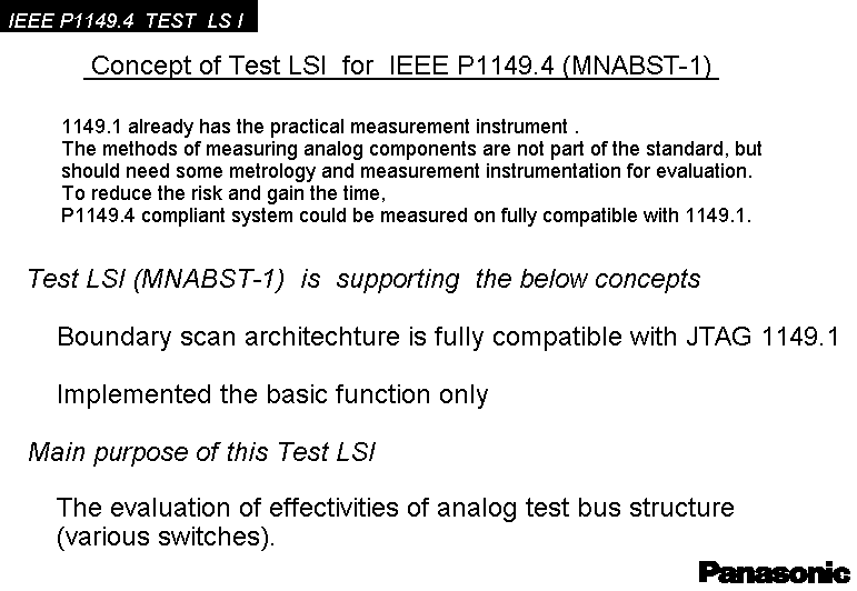
Katsuhiro Hirayamu's (MEI) presentation:
Viewgraph VG13: A 1149.1 fully compatible test
chip has already been fabricated. However, measuring analog components
is not possible with just 1149.1. P1149.4 can be used to solve that problem.
The main objective of this test chip is to evaluate the effectiveness of
the analog test bus structure and its various switches.
Viewgraph VG14: Provides a summary of the features
of the 0.35-um CMOS test chip housed in an 84-pin QFP (0.65mm pitch): 1)
5-pin 1149.1 compatible TAP controller. 2) Two analog test bus ports (AT1
& AT2). 3) Four sets of digital boundary scan input/output ports. 4)
Fifteen sets of analog boundary scan ports. 5) Two control ports for analog
switch impedance in each analog boundary module. 6) One reference for compactor
threshold.
Viewgraph VG15: Internal structure of the test
chip. The core circuitry is the back-to-back inverters. Steve asked if
this has already been fabricated. Katsuhiro said the chip is currently
in fabrication.
Viewgraph VG16: Shows the 5-pin test controller
structure.
Viewgraph VG17: Logic schematic of ABM. The RMODE
port comes after the decoder (4-wire bus). VREF may be adjusted at the
comparator.
Viewgraph VG18: Example of TEST board image.
The test chip mounted on a test board can be inserted into an application
board for test.
Viewgraph VG19: Shows the pin assignment of the
test chip in an 84-pin quad flat-pack.
Viewgraph VG20: Switch impedance is adjustable
in the range of 100 Ohms to 6.4 kOhms. The switch impedances are adjusted
by varying the voltages.
Adam asked when we'll get the test chip. Katsuhiro said by ITC. A letter was given to the Working Group detailing Matsushita's intentions:
Requirements for P1149.4 Test chip and documentation: It is the intention
of Matsushita to contribute to the efforts of the boundary scan project
by supplying tools and documentation to aid in P1149.4 development. For
that purpose, Matsushita will make available to the WG a test chip and
documentation. To receive this package, Matsushita must receive instructions
from export control on the Japan side and non-disclosure agreement (NDA)
on the US side. It is envisioned that these activities will occur concurrently,
and to that effect, Ren will draft an appropriate NDA, and upon receiving
a letter of intent on the requesters' respective corporate letterheads,
to Ren's attention, will make available to the requesters of this development
package. Requests should be sent to:
SUMMARY: Matsushita has developed a test chip that is compatible
with 1149.1 and that incorporates analog test busses with switches for
aid in P1149.4 development. Interested individuals may submit their requests
to the above address.
Refer to viewgraph VG21. Only the functional
requirements of the ABM should be ruled. Brian said we'll only show examples
but not actual implementations. Steve said a minimum of 3 bits is required.
Brian responded by saying we agreed on defining the functions only but
not the number of bits. Adam said the issue is for BSDL in terms of supplying
the software with enough information for test. Ken added that we would
want to use the same 1149.1 software and build P1149.4 software on top
of it which has always been his intention. The 10/20/95 E-mail on a 3-cell
design is an example of the potential to use 1149.1 software for P1149.4.
Ken said anything can be done but questioned whether we want to do extra,
unnecessary work. It should be noted that if people wanted to add extra
bits, then additional work needs be done for the software. CJ Clark suggested
deferring this discussion until the topic is discussed later in the meeting.
His opinion is that he has no problem with the multiple bits and didn't
see the 3-or-4 bits as a big issue. But Ken said we need to nail down the
number of bits and along with it make a table (need a solid definition
of what they do). 1149.1 has lot of different cell designs. Ken advocated
the preservation of the 1149.1 paradigm, which took 5-6 years to develop.
In his 10/20/95 E-mail message, Ken said using this 3-bit cell design,
he can implement 1149.1 software which would perform simple interconnect
tests without modifications. CJ said a scheme with 3 or 4 bits is fine.
Why restrict hardware people when they can ask software people to make
changes. Steve asked if a chip is 1149.1 compliant, can we say the 1149.1
BSDL can be run on it? Ken said we ought to be able to.
Keith proposed a motion: The number of bits will be 2 for simple interconnect
test (data and control) and one or more other bits will have safe values
defined for 1149.1 mode (simple interconnect). Discussion followed. Ken
suggested orthogonal digital and analog bits. Ken wanted to avoid the 1149.1
predicament in which various flavors of 1149.1 cell design prompted the
need to write a lot of software for them. Ken said the fundamental point
is do we want the digital and analog to be orthogonal? Brian referred to
Table 2 in the draft. We were talking about analog pins. If orthogonal,
we can use digital for analog pins for simple interconnect test and use
analog for analog pins. The goal of this discussion was whether we want
to nail down the number of bits for BSDL's sake. Nobody has come up with
another alternative. The point is Lee would like to see distinct orthogonality
whereas in the draft it's not so. With no resolution imminent, it was decided
to defer the issue to E-mail where Lee will also be involved.
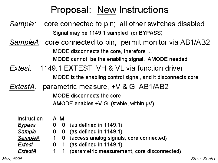
A proposal was brought up concerning the "APROBE" instruction.
In the last WG meeting, Ken's E-mail on this subject was discussed. There
are two versions of Ken's E-mail and Steve disagreed with the contents
in both. Steve's recommendations: (refer to viewgraph VG3),
SampleA is the generic name for APROBE. AMODE is the instruction for selecting
a clean VH, VL, and crude +V and G. The difference between SampleA and
ExtestA is that the latter has core disconnect whereas SampleA doesn't.
But both do allow analog busses connected under control of register bits.
Steve said ExtestA must have very stable voltages. It's an easy sell because
it comes free with the existing bits. Keith said the number of bits is
not a big issue but the number of pins is. Ken asked if VH and +V have
the same function; why need 2 distinct instructions. In 1149.1, Sample
and Extest are the same but here we're "divorcing" the two. Ken
said these two instructions can be merged. He said the G switch must be
able to conduct the current injected. We can merge the two instructions
if it's just voltages we're talking about here. We have to explain to the
user when the two instructions can be legally merged to save bits. Steve
then proposed that the contents of viewgraph VG3 be motioned in. We're
adding two new instructions to what we have already had. Ken said there
are 2 flavors to Extest: strong drive vs. weak drive. We're preserving
what we have and just adding new instructions. Additional decoding is needed
at the pin if VH and VL are different from +V and G. The drive strength
and stability of Vmin and Vmax voltages are of concern here.
MOTION: Contents of viewgraph VG3. Seconded. Yea: 7. Nay: 0.
Abstention: 0. Unanimous approval.
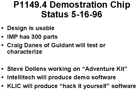
Test chip updates. Keith hadn't seen the February minutes. These test
results were as of 5/16/96.
Viewgraph VG22: The design is usable, IMP has
about 300 parts. Craig Danes of Guidant will test and characterize the
devices. Steve Dollens put together an "Adventure Kit." Intellitech
will supply the demo software. KLIC will produce "hack it yourself"
software.
Viewgraph VG23: Two papers have been accepted
for ITC. Demo paper: need help characterizing part. Early Capture paper:
building a more impressive experiment. Laptop-based demo available. Could
use better test equipment.
Viewgraph VG24: What is working on the chip:
Four isolated boundary cells. Many internal tests. TAP and analog interfaces.
Two differential amplifiers, one with boundary cell and one unloaded. Early
capture extension.
Viewgraph VG25: There were some problems. Boundary
cell 4 meets specs but is "weird." Other 4 cells are fine. Status/control
register has flaw but we can work around it (will change mask on the second
layer for the chips). Swapped state codes in differential cell. All defects
have software work-arounds; chip is fully usable as is. Adam asked CJ if
he understood the controller flaw and knew what to do with it. CJ replied
that he will figure it out.
Viewgraph VG26: A 4x8 board includes 2 demo chips
in zif sockets, one 74CBT244 boundary scan octal, 36-pin Centronix-style
connector, lots of jumpers, and 2x3 perfboard for experiments. Any feature
desired to be added on test board, let Keith know and he'll take care of
it.
Viewgraph VG27: PC-based software. Intellitech
will produce a canned demo that will highlight the Standard and its capabilities.
KLIC will make available "the source code of user-fiendish software
suitable for hacking together user experiments." Keith needed to know
who will do it on PCs and who will do it on a tester. CJ asked if Keith's
board is flexible enough to change the connector pinouts. Since CJ already
has the software, if the pin-out is compatible, one can just plug Keith's
board in their system and test it.
Viewgraph VG28: Availability. Steve Dollens will
work out a purchasing mechanism at IMP. The boards will be at cost, "a
few hundred" dollars. How many more chips and boards should we make?
For the chip, Keith provided a floppy disk that contains the document for
posting on the SPA system.
Viewgraph VG29: KLIC action items. More characterization
data are needed. Build high-speed Early Capture interface. Finish demo
software and ITC papers. Whoever helps Keith to characterize needs to give
data to him before the ITC paper deadline. This is a wonderful opportunity
to showcase P1149.4.
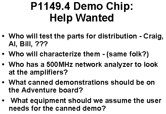
Viewgraph VG30: Help wanted. Issues already discussed
last meeting. HP offered their Portland facility where a network analyzer
is available for Keith to use. He needed to define what the user needs
to do to get what he wants. Adam said CJ's tasks are different from what
Keith wants to do. This issue will be discussed later.
Viewgraph VG31: Even more help wanted. ESD testing
and ATMS option need study. Keith wanted to limit the number of instructions
to be demonstrated and will take this up with Ken and Steve.
Steve Sunter had prepared a list of tests and
those responsible for testing the demo device.
CJ reported that the demo software is about two months behind everybody
else. It will be a windows-driven interactive program complete with pull-down
menus, dialog boxes, etc. CJ showed a viewgraph
of a partially completed top-level menu and associated windows. The components
U1 and U2 on a test board will be based on Ken's BSDL. A second viewgraph
showed the underlying layers and menus in U1. A limited number of instructions
will be built into the software for each of the U1, U2, and U3 devices.
CJ will insert a table found in the draft in a menu that is user-selectable.
The user will have the flexibility of enabling and disabling different
combinations of switches (all 11 choices will be available). But at the
moment, the software was lagging the hardware. CJ commented that the software
will be flexible enough to adapt to any chip. Bill Coombe offered to provide
hardware from Craig Danes to CJ so CJ could wire it up and test his software.
It was pointed out that Keith's own test board is different from Dollens'
board circuit design. Adam suggested putting company logos in the beginning
of the software as "payback" (advertisement) to CJ and other
participating companies for the software work done for the WG. Steve asked
if anyone has measured a resistor. Bill said no. They had just gotten started
last week. Bill also asked for a list of people who will help out with
testing the test chip.
Variable Vref: Steve Sunter replaced the topic "Additional Test Scenarios," which was already a "done deal," with "Variable Vref" (viewgraph VG5) and "4-vs-3 latches" (viewgraph VG6). The variable Vref was motioned and approved by the WG in February, 1995. It is useful for extended interconnect. For some ICs, Vref must be pin-selectable (non-overlapping ranges). We've mandated it must be dc and be available to AB1 & AB2. Does it have to be internally generated? The fourth and fifth bullets on the viewgraph are reasons for the variable Vref. Keith said we can use a comparator to get around the problem of selecting variable Vref. This possibility changes things significantly. Steve said he has to think about this a little more.
Four latches in less area & clock cycles than 3? The new scheme
will take less area than the old one. Fewer scan bits are required and
more control is possible. This proposal is probably too late to be incorporated
into the Standard. But Steve was just trying to bring to the WG's attention.
This is not a new idea since 1149.1 also considered it.
Ted Eaton requested to be on the ballot. Adam will add his name to the
ballot list. The ballot request has gone out -- 45 days for reply. Balloters
are requested to read the draft and put comments on the reflector. Ken
said the figures and drawings are important and are intended to be just
examples of implementation but are not rules. CJ asked for a time frame
for the draft. June, 1996 was the original plan for the ballot. But it
was optimistic. Steve said we can edit, proofread, and tweak the draft
all we want but it needs to go out for comments and insights that we may
not already have. Adam put the number of ballot people at 75 in addition
to however many other names the IEEE may add to it. An estimate of the
number of balloters is 200.
Keith wanted to discuss the variable Vref on the E-mail. Steve tried
to solicit comments from the WG, saying we're going for the final draft
here.
Keith will have his ITC paper reviewed by the WG. Keith asked if anybody wanted a copy of his current draft of paper. Ken and Steve said they do.
The next meeting will be held at ITC in Washington
D.C.
Since at this time the WG was ahead of the schedule, there was suggestion
of going over the draft again. But the topic of discussion shifted to voting
rules in the WG. Steve objected to the relaxation of the rule for becoming
a WG member with voting privileges and argued his case. Steve said we have
set the requirements to avoid being in a situation in which people with
superficial knowledge were allowed to vote, resulting in longer and less
productive meetings. Steve added that the technical materials take a long
time to digest. Other WG members felt that an exception to the rule should
be made for Matsushita. Matsushita has obviously demonstrated more than
a superficial knowledge by building a P1149.4 demo device. They also sent
representatives to the last meeting.
MOTION: It is proposed to suspend the existing rule to vote in the
WG to allow Matsushita Electric Industrial, Limited, (Panasonic) to participate
in the voting process without fulfilling the requirement of attendance.
Seconded. Yea: 7. No: 0. Abstention: 1. Motion carried.
Seconded. Unanimous approval. Meeting officially adjourned.