| Time | Topic | Responsibility |
|---|---|---|
| 8:00am | Arrival and Introductions | Adam Cron |
| 8:15am | Approval of June, 1997 Minutes | Adam Cron |
| 8:30am | CD State | Adam Cron |
| 9:00am | Pin Catagories | Keith Lofstrom |
| 10:30am | Break | |
| 10:45am | Pin Catagories - continued | Keith Lofstrom |
| 12:00pm | Adjourn for Lunch | |
| 1:00pm | Differential Issues | Keith Lofstrom |
| 2:30pm | Anatomy of a Pin | Keith Lofstrom |
| 2:45pm | Break | |
| 3:00pm | Example Circuits | Keith Lofstrom |
| 3:45pm | 1149.1 Status | Ken Parker |
| 3:50pm | Next Meeting | Adam Cron |
| 4:00pm | Adjourn | Adam Cron |
| 4:05pm | Subgroups for Wordsmithing | Adam Cron |
| Working Group Members | 31ish |
|---|---|
| Total Subscribers | 426 |
| Total Subscribers on "esd" reflector | 429 |
| Countries Participating | ~32 |
| Companies and Other Institutions Participating | ~250 |
| Funds Available | ~$550 |
| Name | Company Sponsor |
|---|---|
| Adam Cron | Synopsys |
| Firooz Farhoomand | Matsushita Electric Corporation of America |
| Keith Lofstrom | KLIC |
| John McDermid | Hewlett-Packard |
| Elbert Nhan | Johns Hopkins University |
| Ken Parker | Hewlett-Packard |
| Steve Sunter | LogicVision |
| Brian Wilkins | Southampton University |
| Name | Company Sponsor |
|---|---|
| Mani Soma | University of Washington |
Adam said the Tiger team met on Saturday and Sunday (8/22 and 8/23) from 10:00am to 7:30pm each day discussing the differential issues, the draft, etc. Steve Sunter maintained notes of what transpired during the Tiger team meetings.
Adam asked that Steve Sunter give a summary of the meeting notes:
Adam heard a motion to approve the 1997 ITC meeting minutes. Steve seconded. Unanimous approval.
Adam made changes to the meeting agenda. The Working Group will break into subgroups later to work on separate topics.
One of the issues discussed during the tiger team meetings is coming up with an unambiguous term for the condition under which a pin is in a "quiescent" but not strictly a "High-Z" state. This quiescent state is not the same as a High-Z condition in the digital terminology. The condition is such that no dependent AC or DC sources are driving the pin but that there may be a 50-ohm resistor connected to it.
A pin is in this state may be internally "driven" as follows:
The fourth condition above was originally "can be modeled by a linear or piece-wise linear system." Steve questioned whether that included everything since any system can be linearized. But Keith said the piece-wise linearization is valid over a certain range of interest where the approximation holds. Further discussions resulted in the words "piece-wise linear" being deleted from the original wording (see viewgraph VG1). Steve said this definition is fine but wondered whether the designers were going to be comfortable with something nonlinear such as a diode hanging at the pin. John McDermid said we could model a nonlinear component such as a diode in the "off state" by a capacitor (see VG1). So the phrase "linear through the range of measurement interest" was therefore added.
When a pin is in a state that satisfies the above requirements, what should the state be termed? Two suggestions were "N-State" and "Q-state," both of which have other connotations. Brian then suggested "CD-state" because that is essentially what it is. Even though the moniker consists of 2 letters, it is an unambiguous term. After further discussions, a motion was initiated.
MOTION: A pin is defined to be in the CD-State when it meets the following conditions:Motion seconded. Unanimous approval.
Keith added that a pin in "CD-state" could also be in a "High-Z" state when its in the "CD-State" since one option for the "CD-state" is the "High-Z" state.
Since we have just settled on the term "CD-state," it will be used in Chapter 3 and everywhere else in Draft. Ken said it was worth taking a little time out to work on the definition of a "CD" state.
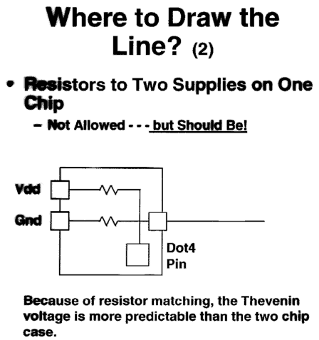
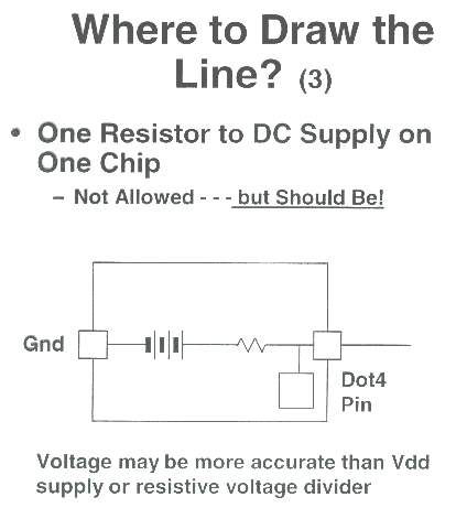
Keith presented a set of slides which were made prior to this meeting. So, where Keith says that an item "is not allowed", it may now be allowed.
Adam drew a picture showing various impedences, and noted whether or not they were allowed, and when they must be documented.
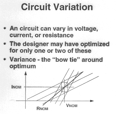
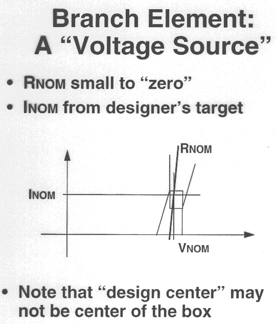
Keith put additional viewgraphs up on "circuit variations." Keith pointed out in VG13 that a given circuit can vary in voltage, current or resistance and that the designer may have optimized only one of these quantities in his design. This results in a "variation window" around the optimum point that has to be taken in account. VG14 shows how a current source can be modeled. A voltage source can be modeled as shown in VG15. A proposed branch element (VG16) is that a combination of both a current and voltage source models a pin that captures and encompasses variations in R, I, or V.
Keith commented it all comes down to modeling and that we need to talk about what is correlated to what. VG17 describes the sources of variation. There are two types of impedance. One is a resistor and the other is linearized resistance from other sources. This requires a way to correlate the impedances. John said designers need to reduce circuits to those branch elements to facilitate testing. Ken said the verification process is important. What we should do is reduce circuits to technology independent "Black Boxs" (VG18) and take into consideration variations in circuit parameters from the system to the chip level. More accurate tests can be performed if variations are quantified.
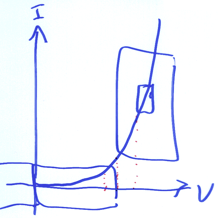
Whats the range of validity (VG19)? There are a couple of factors limiting the practical range of validity: 1) valid over a small range, and 2) parts have "absolute maximum" ratings. Limits may be included in the branch descriptions. Designers have to consider these issues and they are being asked to think more about the testing aspects. Hopefully, it will all be automated. Steve said still, it might not be a simple task to model everything in a design by R, L, C, I, and V since tools that generate models dont exist yet. Keiths presentation is on tolerances but why consider tolerances, Steve asked. The purpose is that we would know what we are measuring instead of what we think we are measuring. Ken was worried about the potentially huge amount of documentation for a pin.
Steve was concerned about the valid range of measurement. He said basically there are two modes of EXTEST with and without off-chip termination. We need descriptions for both cases when in core-disconnect. Adam asked if we can come up with just one that contains both pieces. Refer to Keiths viewgraph (VG20) depicting a transistor connected to a pin with an off-chip 50 Ohm terminated in 2V. John asked if we can do any meaningful measurement with the termination resistor off-chip. Keith said yes. Steve asked what will be seen if a +/-100 uA current is sourced into the pin. Keith said the range of validity is constrained to that within which the device will operate normally. Keiths intention is to simplify the process. All we really care about is where the device will function normally and not anywhere else. In VG20, if the base of the transistor was tied to the positive rail, then the emitter pin will look like a diode (bottom graph). An automated tool or program can be used to model it. John and Ken were wondering if we will need this for most of the pins we deal with. Maybe for a very small fraction of the pins we would need this. Keith reminded everyone that chips are really nothing compared to the complexities of boards. Most of the difficulties arise from off-board testing and not off-chip testing.
Steve said maybe its the test engineers job to determine which model to use and there should be a default model. Adam then asked Keith what we should do so Brian can put it in the Draft. Keith said we should use a default model first (a complete disconnect) and if that doesnt work, then we go to another model. The designer needs to provide a default model. There should be an algorithm that determines an appropriate model for a particular operating point of interest. The question now is how many of these linear pieces we will need. John said not to worry about having too many linear pieces but rather we should develop a few additional models besides the default depending on the situation, design, etc.
On an example I-V curve shown in VG21, Keith stated that only the ranges demarcated by the rectangular boxes will be considered valid. Any point on the curve outside the boxes should be flagged and labeled "invalid." Steve suggested that we need closure on this topic and should move to another topic. We can continue this discussion over e-mail. One of the conclusions is that the new CD state does NOT warrant a new definition for a VREF pin.
Keith showed various examples of integrated circuits such as an analog switch and others that we dont need core disconnect for. For a simple analog switch, we get a CD switch "for free."
Power supply pins dont need an ABM. Function pin: Steve said the definition of a function pin is that it is a pin that "conveys data in and out of the chip." Are the definitions of a power and function pin good enough? Steve and Brian both think so. Were trying to prevent esoteric and unusual cases, and thats not practical. Whats the difference between a power pin and other pins? Keith said nothing works if power pins are not limited. If we say a power pin conveys power onto the chip, then Vref fits that description too. Ken said the power pin definition is a non-issue until now when we are trying to define Vref. Keith said its a "soft spot" that we need to look carefully at. Lets leave the definition of a power supply pin. Brian said nobody needs a power supply pins to be defined. Steve said we just need to say whether a pin is a power supply pin. Keith disagreed. Keith said we should say something like "a function pin includes input, output, functional, etc." In other words, he favors a list that enumerates the different functions. Ken said Vref does contain information and data. Steve was opposed to a list since it can keep growing as we can always find new things to add to it. Brian suggested adding to the end of the definition of a function pin something to the effect of "most pins except the power supply pins are function pins." Ken agreed. Keith said we need to mention somewhere that Vref pins are NOT power supply pins.
Among the many examples of commercially available integrated circuits is Analog Devices AD7524 DAC. There is a "RFB" and a "VREF" pin on the chip. There is no difference between those two pins since both are considered "mission" pins. Since this is a multiplying DAC, VREF is no longer stable or constant. Ken asked, for this example, which pin we should put an ABM on. Lots of them do not need ABMs. Ken said it would be a good exercise to take one of these existing integrated circuits available on the market and try to apply Dot-4 to it. Any resistor or passive component used on the chip will need to be documented if it cannot be absorbed as part of the core or mission circuit.
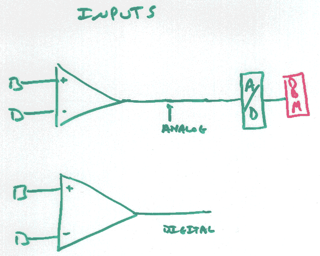
On VG22, Ken asked how the data at the output that is captured by a control flip-flop, fits into the scheme of Dot-1. Ken said if we took one of those flip-flops that controls AB1 and AB2 and have it capture the result, then it will fit into the Dot-1 scheme. Steve said that this is an analog circuit. If the differential buffer was analog and we wanted to support INTEST, then wed need to capture the input to the buffer (VG23). If it's an analog circuit, theres no INTEST, and therefore no capture is required at the input to the buffer. If a digital buffer, then we would need a DBM. On VG23, Ken said we need to draw 2 lines for the 2 inputs to the differential buffer. Steve said the two outputs must never be both 0 or both 1 simultaneously. We would need to document it if it is unavoidable or necessary.
BSDL can identify the + and - pins of a differential buffer. Brian will draw these diagrams up. The control and logic and gates will supply the Vh, Vl, etc. Steve asked if we need to capture the difference between the inputs? Keith wanted a permission for that possibility since a lot of folks will find this a useful things to have.
Existing BSDL software doesnt know how to handle situations where somebody hangs a differential driver (see VG23) at the output of the differential buffer and the output of the driver is sent to a control cell like Ken suggested. Anytime you put more flexibility to software, it becomes more complicated.
Adam said its ad hoc and we shouldnt really worry about it. So lets leave the driver out for now. Steve said if we decided to put it in, then make it a rule. Dot-4 software that hasnt been developed can provide special diagnostic software. Ken suggested that when this all gets written up, we should send a copy to Adam Ley since there will be significant differences between Dot-4 and Dot-1. Ken asked whether or not we have described the differential capabilities well enough for us and them to understand it. Do we really understand it?
Keith said another issue is if we wanted to support INTEST, can we stimulate the core? The way the input differential buffer is drawn we cannot support INTEST. Wed need to add a DBM in front of the core (see VG22). Steve thought we always require a DBM. Its just an observe-only DBM. The designer can add a comparator (in blue on the viewgraph) which may be required. Are we dealing with implementation details here? The designer should have this flexibility.
Ken said what is differential in test mode may not be so in normal operating mode. Steve said Dot-4 doesnt state that we need a DBM at the digital differential output. In Dot-1, its required. Steve said John Andrews should resolve this issue in Dot-1.
Adam again brought up the issues regarding the input receiver differential buffer. We always capture the difference between the inputs. But on the output differential buffer, Steve said if we talked about digital differential drivers, then a DBM may be required in front of the combination logic and gates. Now the DBM at the inputs of the differential output buffer can be eliminated.
In VG22, the "blue" receiver is there for some cases that the "red" DBM cannot accomplish. Now in VG23, the red DBM is at the front end and the question is should we require (if so, make it green) the blue receiver or leave it blue? Keith wanted to see the comparator there and it probably wont cost that much more. He thinks its going to be more expensive to create the flip-flops than the multiplexers provided the noise is not too much at the comparator. Adam didnt feel we have enough people here to make it a motion. Lets make it a recommendation.
It basically comes down to the question of a tradeoff between symmetry vs. simplicity in architecture (elegance of architecture or minimizing the number of bits).
Adam put viewgraphs VG24 (Inputs) and VG25 (outputs) up and asked where we should sample the signals? John asked why we want to sample. Because we want to know the difference between the inputs and that can be done by hanging a comparator across the inputs or a single-ended comparator at the output of the differential buffer. You can then compare the output with the mid-rail or some other reference but it would not be possible to detect small signals in the mV. Keith said putting a comparator in there is guaranteed to be useful. He said hed like more chip functions than saving silicon real estate or hardware. The DBM at the output in VG24 is for INTEST. Thats still the case here. Adam asked where the comparator should be placed in the diagram. He pointed out in VG25 that Dot-1 says you must capture at the inputs and outputs of the "output" differential comparator. The capture point of the cell can either be the input of the buffer or at the output. We dont want to mandate the extra hardware and also sacrifice the performance of the cell if we sampled everywhere. So which, the input or the outputs would you rather capture? The data at either capture point will go to the same control flip-flop.
Adam is concerned that he would have to explain to the balloters that weve made significant changes to the differential capability. If 93% of the people said its fine with them that the comparator is not there, then why should we bother with it.
Keith suggested putting a comparator at the outputs and sending it to the AB1 control flip-flop.
MOTON: For an analog output pin, a comparator is required at the outputs. Seconded. Unanimous approval. Motion carried.
MOTION: It is mandatory for the digital output pin to have an observe and control comparator. Seconded. Unanimous approval. Motion carried.
For an input pin, everybody pretty much agreed with it. Therefore, no motion was initiated on that.
Keith suggested that we read a data book and see what the engineers are currently working with. Ken asked if the circuits that Keith were showing are highly utilized. Keith showed a Micro Linear A/D converter. Reference resistance is not to ground. So that would be a documented resistance. How do you turn off the 10V internal reference? Its an independent DC source. Other examples were mixed signal parts. Keith commented that digital designers are "terrible" analog designers and vice versa. These are rather "nasty" mixed signal parts we are dealing with today. There are some circuits that we probably dont even want to bother putting testability in because of their sheer complexity. Theres a Micro Linear part that when put together with a couple of external parts will give you a hard drive. Ken asked if Micro Linear would be interested in Dot-4 testability. Keith said at least Seagate would be interested since disk drives is a highly competitive business. Ken said up to 25% of boards could be taken up by test paths and people dont like that. Keith encouraged reading the datasheets and see what application circuits are out there. Ken said it might be interesting to ask Seagate, Micro Linear and other such companies to a meeting and ask them if theyd be interested in testing their products with Dot-4. This is how we build a consortium. We might even want to throw in an ATE company in the mix. Also, it might be an interesting ITC panel topic to have 2 to 3 disk drive and chip set vendors talk about how to test their products.
Keith asked Brian what if anything he wants us to help him with. He said hed need help on the differential issues as far as tables, figures, diagrams are concerned.
Adam Ley converted chapter 10 into 3 sub-chapters. Ken is reviewing them. Adam is a thorough guy. But progress is slow due to his work commitments.
ITC, Sunday, 10/18/98, from 8am to 6pm in the Idaho room of Sheraton Hotel. Agenda will be determined after Brian edited the draft. Ballot will be done with 3 months from now. We will be in ballot by ITC. Keith has been looking at real circuits and application circuits. We can show people what we have to deal with. Ken will help out with the descriptive part of BSDL. Analogys Ernst Christin, the vice chair of the 1076.1 VHDL-AMS working group on design automation VHDL language is "gung-ho" about Dot-4 and has some ideas about this. He might do a guest spot at one of these meetings.
Motion to adjourn meeting. Seconded. Meeting adjourned.
Steve and John to write chapter 9; Ken and Adam to work on chapter 10, and Keith on differential 7.4.
One other thing Steve said we havent talked about is "the definition of X." Colin Maunder asked about that. We have to document the states, everything except 00 and 11.